Half-Adders
- A half-adder circuit performs one-bit (LSB, least significant bit) addition.
- Look at the truth table where and are binary input bits, is the summation of the two input bits and is the carry out (output carry).
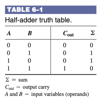
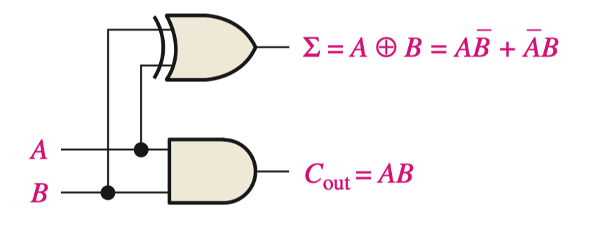
- From this table, we can derive the Boolean expressions:
- This can be implemented using the following logic circuit:
Full-Adders
- A full-adder is used for all binary places EXCEPT the LSB (which uses the half-adder).
- The main difference between a full- and half-adder is that the full-adder also accepts an input carry.
- Look at the truth table where and are binary input bits, is the input carry, is the summation of the two inputs and the input carry, and is the output carry.
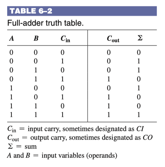
- From this truth table, the following Boolean expressions can be obtained:
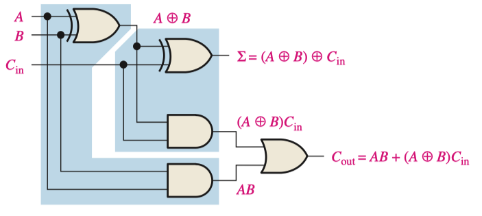
Notice that the full-adder consists of 2-half adders and 1 OR gate
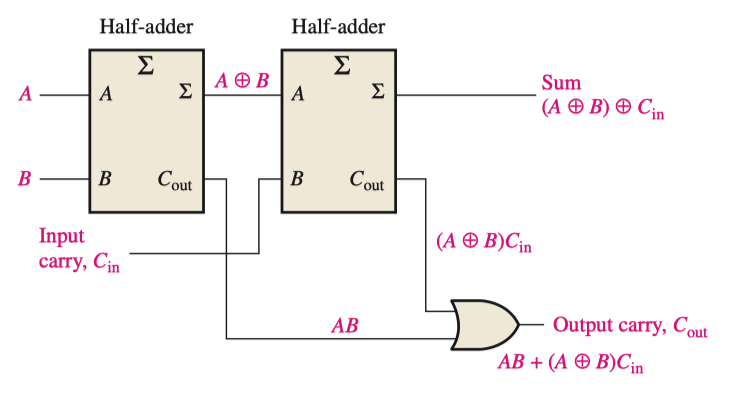
- Full-adder redrawn using 2 half-adders and an OR gate
Parallel-Adders
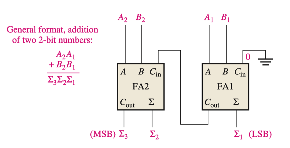
- Two or more full-adders are connected to form parallel binary adders. → Performs addition of several binary digits
- Consider two 2-bit binary numbers ( and ). Two full-adders can be connected as below to form a 2-bit parallel adder that produces a 3-bit result ()
Ripple-Carry Adder
- The previously shown 2-bit parallel adder is an example of a ripple-carry adder, in which the carry output of each full-adder is connected to the carry input of the next higher-order stage.
- The disadvantage of the ripple-carry adder is that it can become very slow when adding many bits, because the carry must ripple (or propagate) through each stage sequentially.
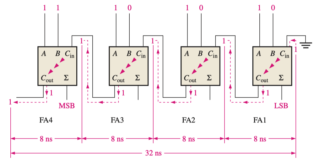
- Full-adder 1 (FA1) cannot produce a potential output carry until an input carry is applied. Full-adder 2 (FA2) cannot produce a potential output carry until FA1 produces an output carry. Full-adder 3 (FA3) cannot produce a potential output carry until an output carry is produced by FA1 followed by an output carry from FA2, and so on.
Look-Ahead Carry Adder
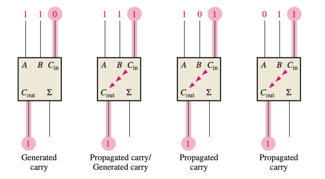
- One method for eliminating the ripple-carry delay is to use look-ahead carry addition that anticipates the output carry of each stage and produces the output carry by either carry generation or carry propagation.
Carry Generation
- The output is produced internally by the full-adder only when both input bits are HIGH.
Carry Propagation
- The input carry is rippled through the adder to become the output carry. This only happens when either or both of the input bits are HIGH.
Output Carry
- The output carry of a full-adder can be expressed in terms of both the generated and propagated carry.
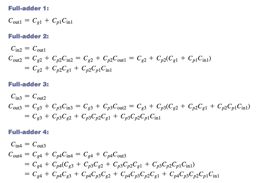
เจ้าหนุ่มหัวใสซักคนนี่แหละ แทนสมการเข้าไป สรุปเห็นว่า the output carry for each full-adder stage is dependent only on the initial input carry () เห็นมะ ๆ มันไม่ต้องรอ Carry อื่นเลย เร็วกว่าแหง ๆ
74LS283 4-Bit Parallel Adder
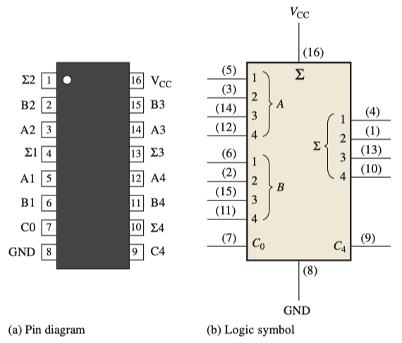
- A commercially available 4-bit parallel adder is the 74LS283 integrated circuit chip that adds two 4-bit numbers.
- It is possible to expand the adder to handle larger numbers by connecting 2 or more 74LS283 chips.
Half-Subtractors
- A half-subtractor circuit performs one-bit (LSB, least significant bit) subtraction.
- Complete the truth table on the right where and are binary input bits, is the difference between the two inputs and is the borrow out.
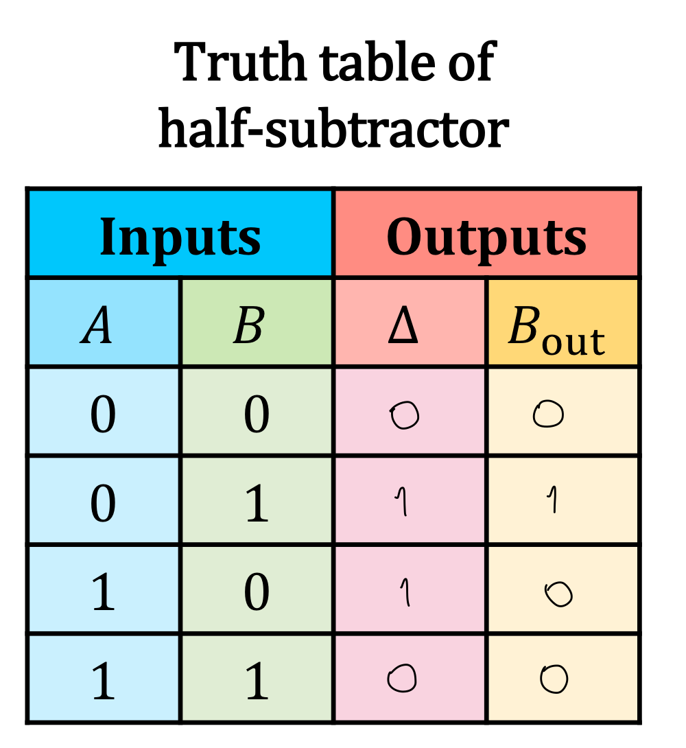
- From this table, we can derive the Boolean expressions:
- Notice that the only difference between the half-adder and the half subtractor is the NOT gate introduced to one of the two inputs to the AND gate.
Full-Subtractors
- A full-subtractor is used for all binary places EXCEPT the LSB (which uses the half-substractor).
- The main difference between a full- and half-substractor is that the full-substractor also considers an input borrow.
- Complete the truth table on the right where and are binary input bits, is an input borrow (borrow-in), is the difference between the two inputs after considering the input borrow, and is the output borrow (borrow-out).
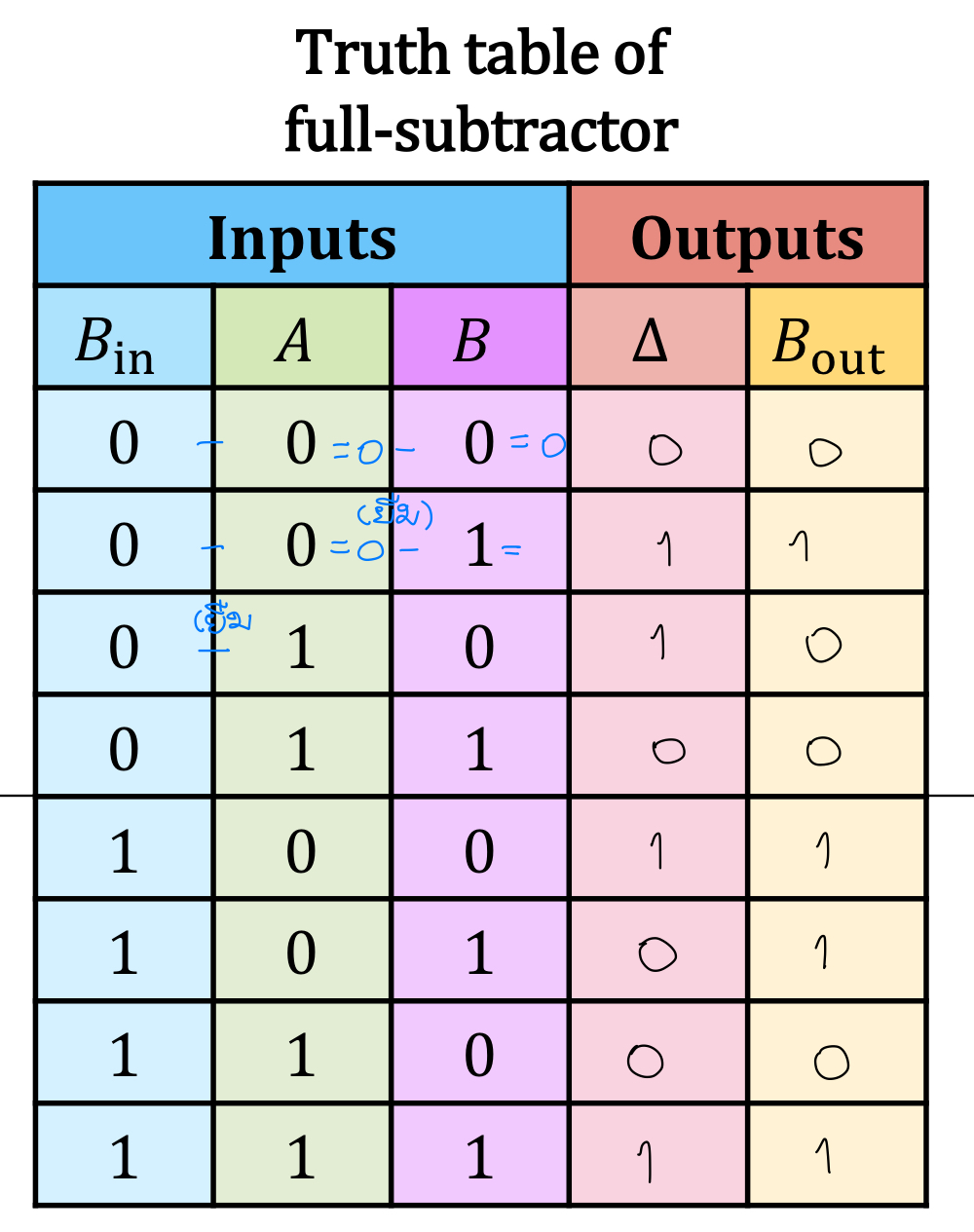
- From this table, we can derive the Boolean expressions:
Comparators
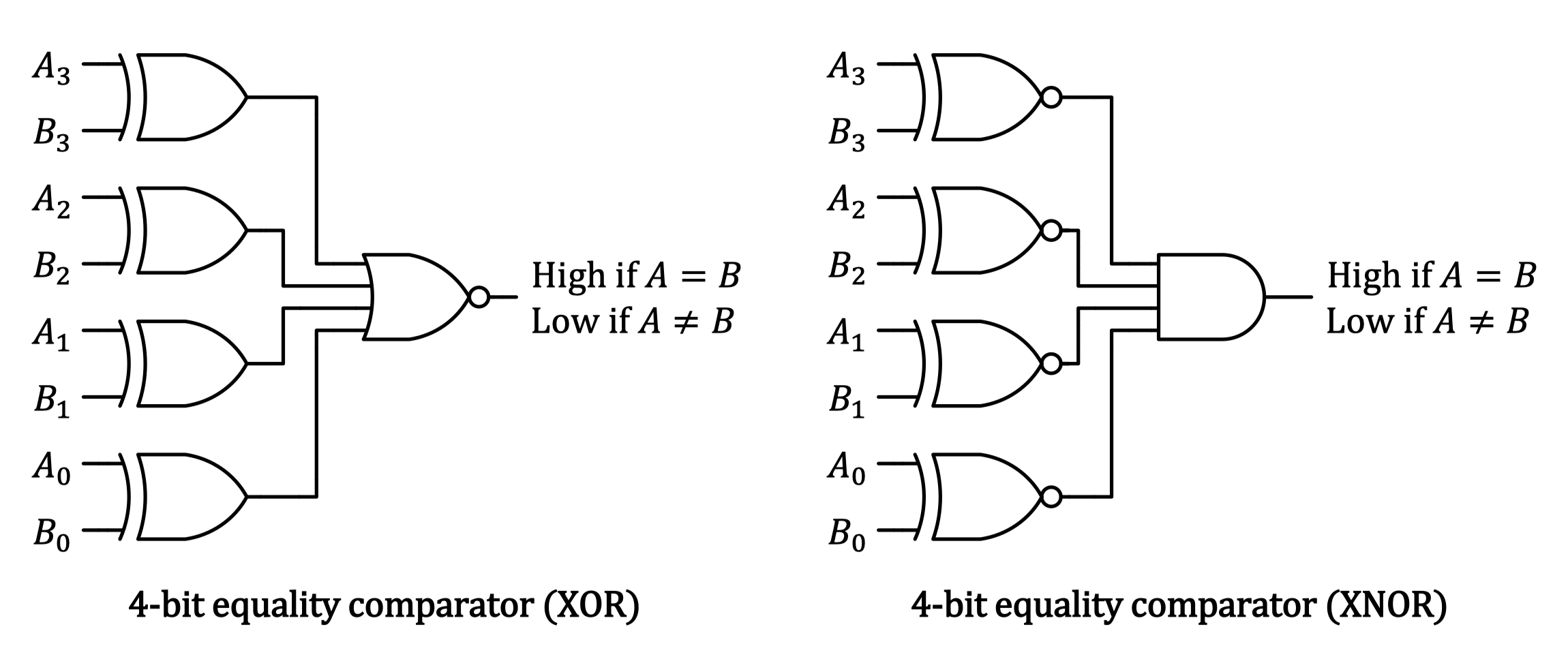
- Comparators are used to compare two numbers, producing an indication if they are equal or if one is larger than the other. It can be implemented using XOR or XNOR gates.
- For two 4-bit numbers ( and ), the following logic diagrams demonstrate implementation of a 4-bit equality comparator
4-Bit Magnitude Comparator
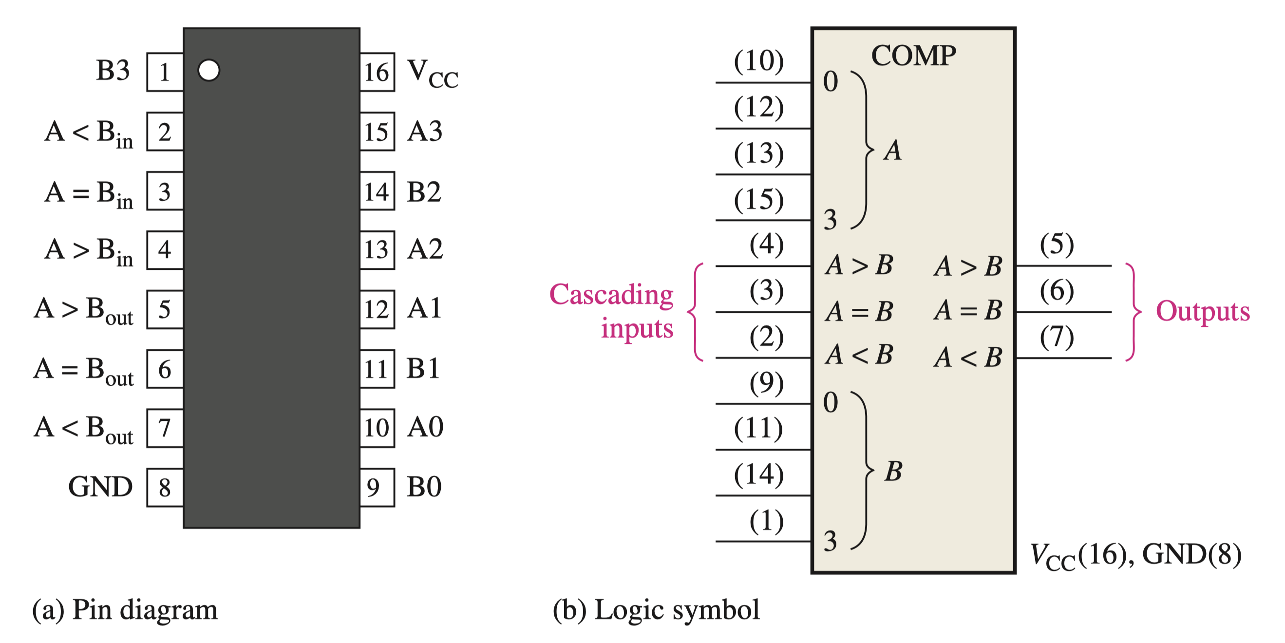
- A commercially available 4-bit magnitude comparator is the 74HC85 integrated circuit chip that determines whether two 4-bit numbers are greater than, equal to, or less than each other.
- It is possible to cascade 2 or more 74HC85 chips for comparison of any number of bits greater than four.
Decimal-to-BCD Encoders
- Encoders convert information, such as a decimal number or an alphabetic character, into some coded form.
- An example is the 74HC147, which is a commercial decimal-to-BCD encoder that takes nine active-low inputs and encodes them into four active-low outputs. This means that only low logic levels (L or 0) on the truth table activate the input, and the active state for the outputs of this IC are also low.
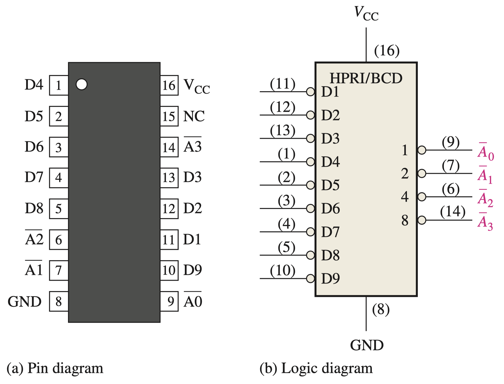
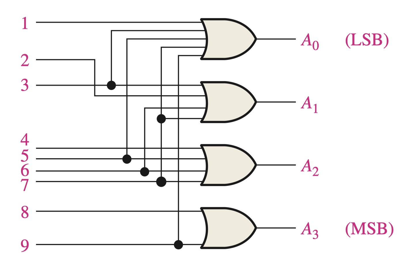
- The logic circuit inside the 74HC147 and its truth table are shown
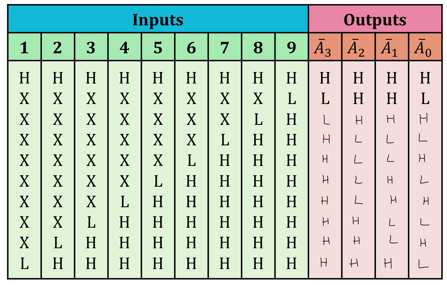
- X indicates don’t care conditions, and define the priority of each input number.
- The priorities are given in descending order.
- For example, if input 9 is activated (L or 0), other inputs are ignored.
8-to-3 Encoders
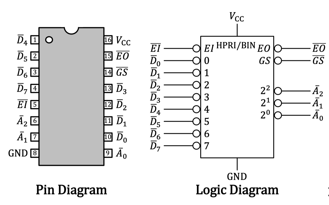
- The 74LS148 is a priority 8-to-3 encoder that converts eight active-low inputs into a 3-bit binary code with three active-low outputs.
- Other control signals include the enable input (), enable output (), and group signal
() that are used for expansion purposes.- For example, two 74LS148 can be expanded to a 16-to-4 encoder by connecting the of the higher-order encoder to the of the lower-order encoder.
Basic Binary Decoders
- A decoder converts coded information, such as binary or BCD, into non-coded form. It performs the reverse operation as an encoder.
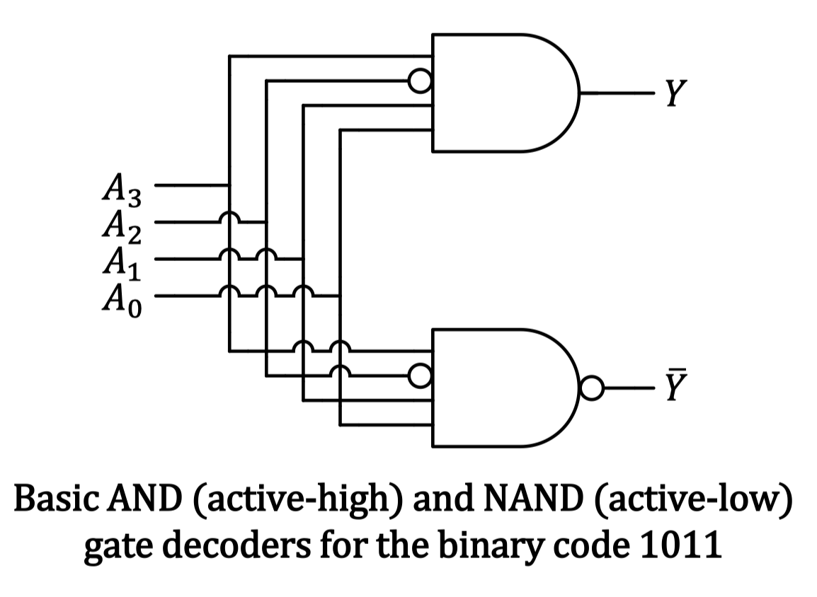
- The simplest decoders detect the presence of a specific combination of input bits or code and output a specific logic level.
- AND gate decoders → produces a HIGH (1) output when all inputs are true.
- NAND gate decoders → produces a LOW (0) output when all inputs are true.
BCD-to-Decimal Decoders
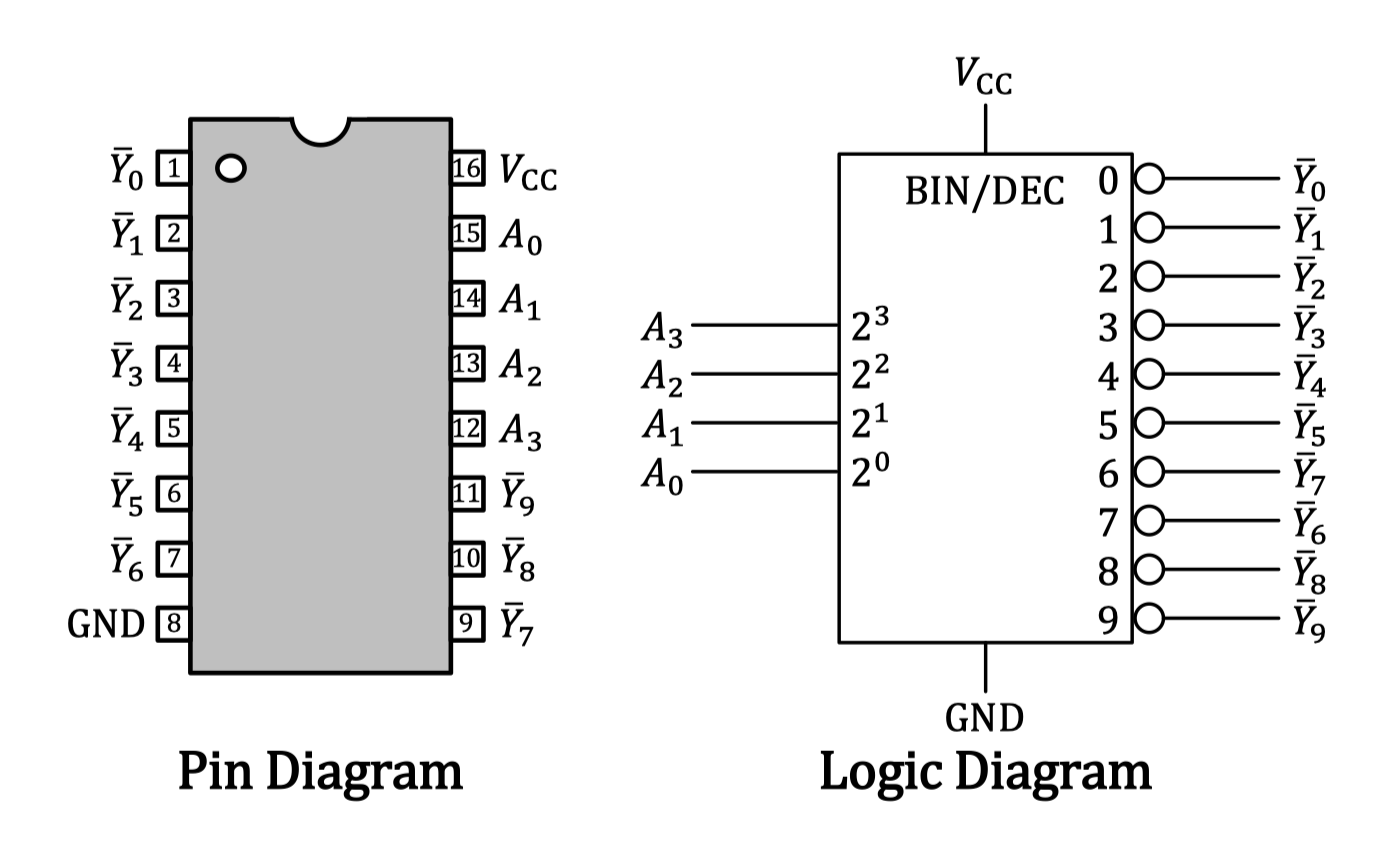
- The 74HC42 is a BCD-to-decimal encoder that converts an active-high 4-bit BCD input and converts it into ten active-low outputs.
- It is frequently referred to as a 4-line-to-10-line or a 1-of-10 decoder.
- The decoding function is implemented using ten NAND gates corresponding to each BCD code to provide active-low outputs.
3-to-8 Decoders
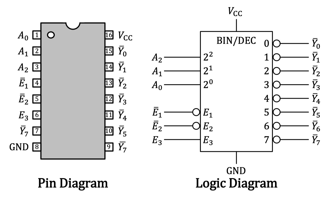
- The 74HC138 is a 3-to-8 decoder that converts a 3-bit active-high binary code into one of eight active-low outputs.
- It has 2 active-low ( and ) and 1 active-high () enable signals
- All enable must be active for the decoder to function.
- The 3-to-8 decoder is one of the more common decoders used in many microprocessor- based systems and is also referred to as a 1-of-8 decoder.
7-Segment LED Displays
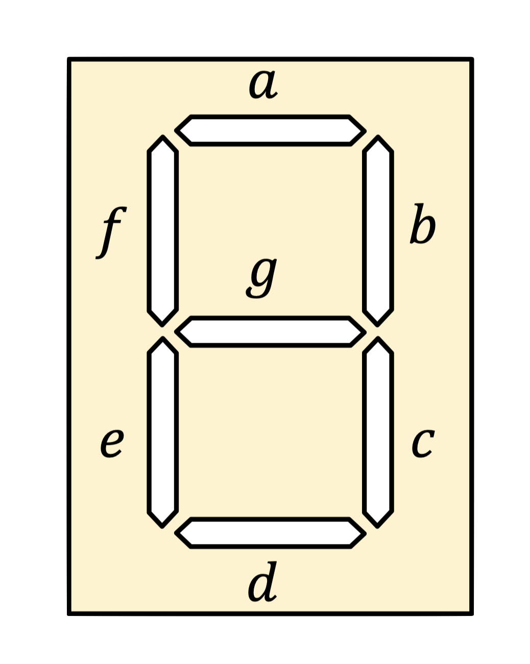
- A common output device to display decimal numbers is the 7-segment display.
- It consists of seven light-emitting diodes (LEDs) that are labeled as through , according to the following figure.
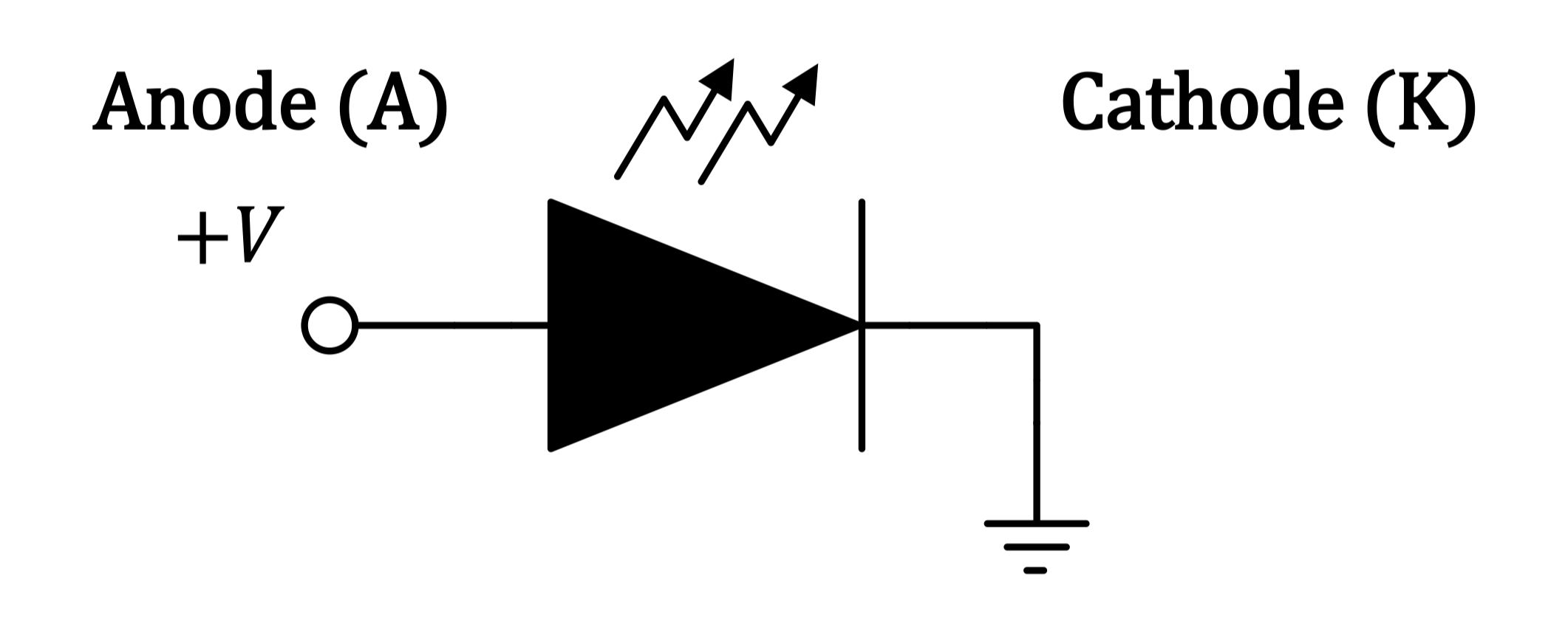
- LED is sensitive to polarity. Hence the cathode (K) must be connected to the negative (GND) terminal, while the anode (A) must be connected to the positive terminal of a power supply.
- The diagram of a single LED is shown below.
- The LEDs in a 7-segment display are not isolated from each other.
- Either all of the cathodes OR all of the anodes are connected to a common lead, while the other terminals are individually available.
- This means fewer electrical connections to the package and facilitates enabling or disabling a particular digit by controlling the common lead.
- ==A common-anode 7-segment display requires an active low device to operate it.==
- ==A common-cathode 7-segment display requires an active high device to operate it.==
- No automatic advantage for each configuration, usage will depend on applications and logic families.
- Depending on the inputs to LEDs a-g, each of the diode is either lit or unlit to form individual digits, as shown above.
- The 7-segment display is normally connected to a decoder that converts a 4-digit BCD number into the appropriate activation signal for each diode.
BCD-to-7-Segment Decoders
- There are two types of 7-segment decoders.
- 74LS47 — produces active low outputs for use with common-anode 7-segment displays. When a segment is activated, the 74LS47 outputs LOW, otherwise it outputs a HIGH.
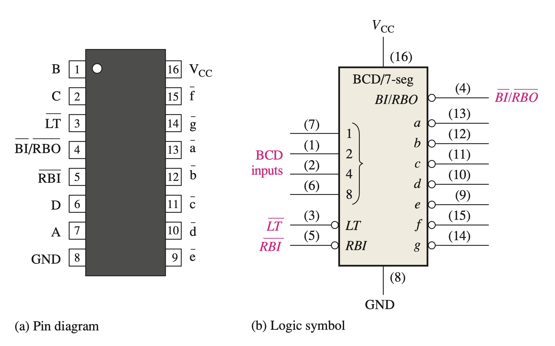
- 74LS48 — produces active high outputs for use with common-cathode 7-segment displays. When a segment is activated, the 74LS48 outputs a supply voltage, otherwise it outputs a ground.
- 74LS47 — produces active low outputs for use with common-anode 7-segment displays. When a segment is activated, the 74LS47 outputs LOW, otherwise it outputs a HIGH.
Multiplexer (MUX)
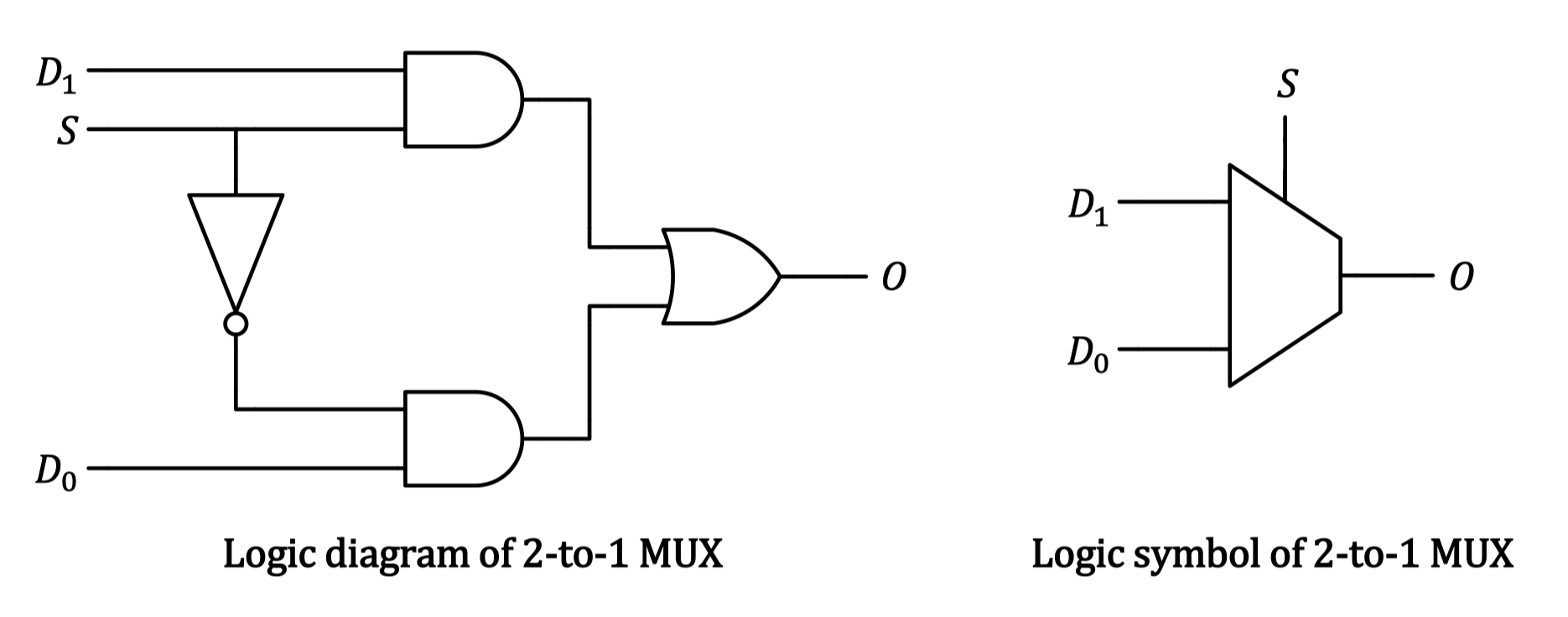
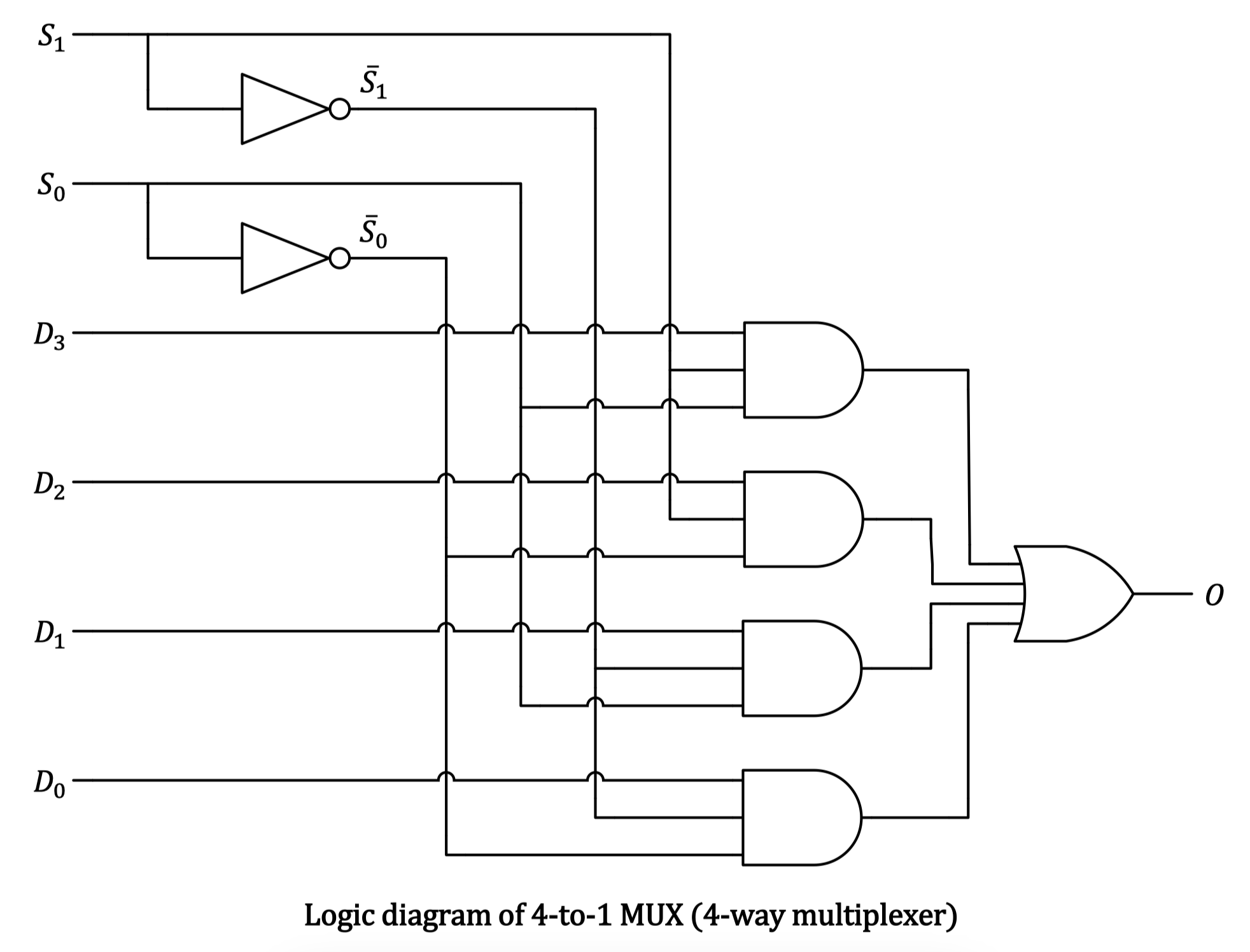
- A multiplexer (also called a data selector or MUX), is a switch that passes one of its data inputs through to the output, depending on a set of select or control inputs.
- Common ICs used to implement MUX is the 74HC157 (Quad 2-Input Multiplexer) and the 74LS151 (8-input Multiplexer).
- A 2-to-1 MUX is shown by its logic diagram and symbol below.
Demultiplexer (DEMUX)
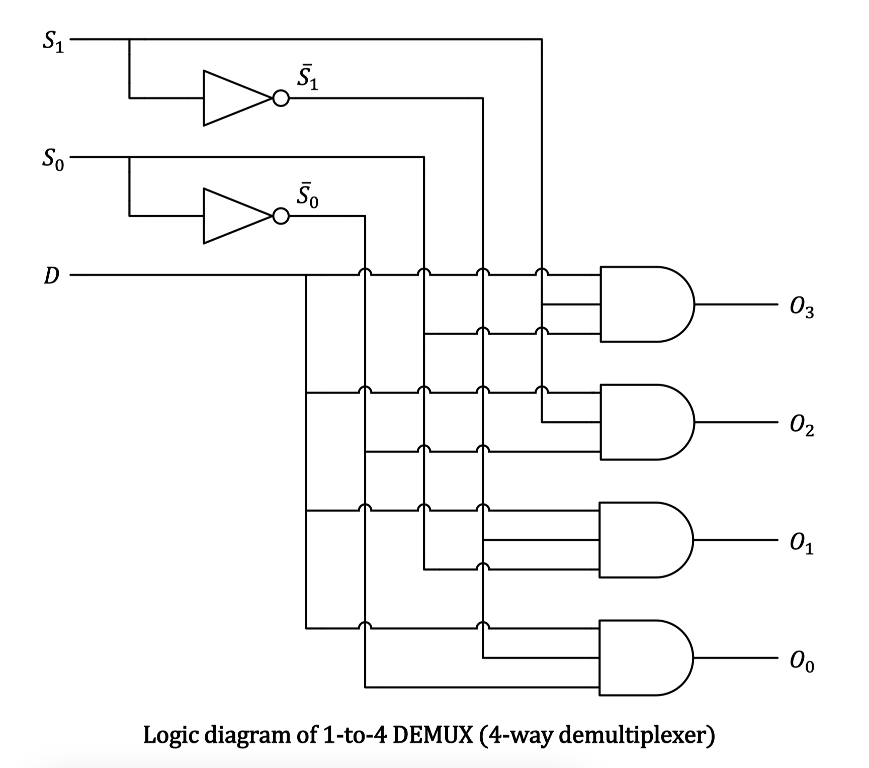
- A demultiplexer (also called DEMUX), performs the reverse operation as the MUX (i.e. it takes the input and distributes it to a given number of output lines).
- A common demultiplexer IC is the 74HC154 (4-Output Demultiplexer).
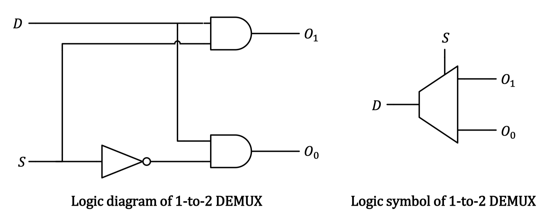
- A 1-to-2 DEMUX is shown by its logic diagram and symbol below: