#Summarized
- Purpose:
- Timer/Counter: Primarily used for counting clock pulses or external events.
- Interrupts: Used to handle events asynchronously, allowing the microcontroller to multitask.
Introduction to AVR Interrupts
Polling vs. Interrupts
A microcontroller can execute only one instruction at a time, but it must handle multiple devices. There are two approaches:
- Polling – The microcontroller continuously checks a device's status and acts when the condition is met. However, this wastes CPU time because the microcontroller cannot perform other tasks while waiting.
- Example: In Lecture Note 7, we used polling to monitor the TOV0 flag in the DELAY subroutine.
- Interrupts – Devices notify the microcontroller when they need service by sending an interrupt signal. The microcontroller pauses its current task, services the interrupt, and then resumes its previous operation.
- Example: A timer interrupt allows the microcontroller to handle other tasks while waiting for a delay.
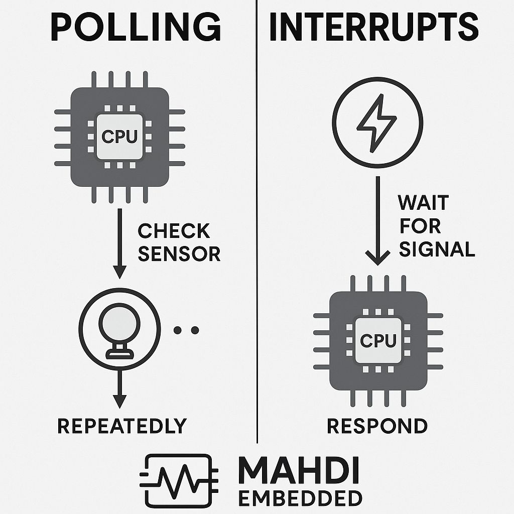
- Example: A timer interrupt allows the microcontroller to handle other tasks while waiting for a delay.
Analogy: Waiting for Mail
- Polling: Constantly watching the door for the mailman.
- Interrupts: Doing other tasks until the mailman rings the doorbell.
Interrupt Operations
Interrupts originate from various sources. The sequence of operations is:
- The interrupt controller sends an interrupt signal to the microcontroller.
- The microcontroller saves the current instruction address (PC) onto the stack.
- It then loads the interrupt-specific address from the interrupt vector table into the PC.
- The instruction at this address directs execution to the corresponding ISR (Interrupt Service Routine).
- The ISR executes and ends with
RETI(Return from Interrupt). - The microcontroller retrieves the saved PC address from the stack and resumes execution from where it left off.
Interrupt Vector Table
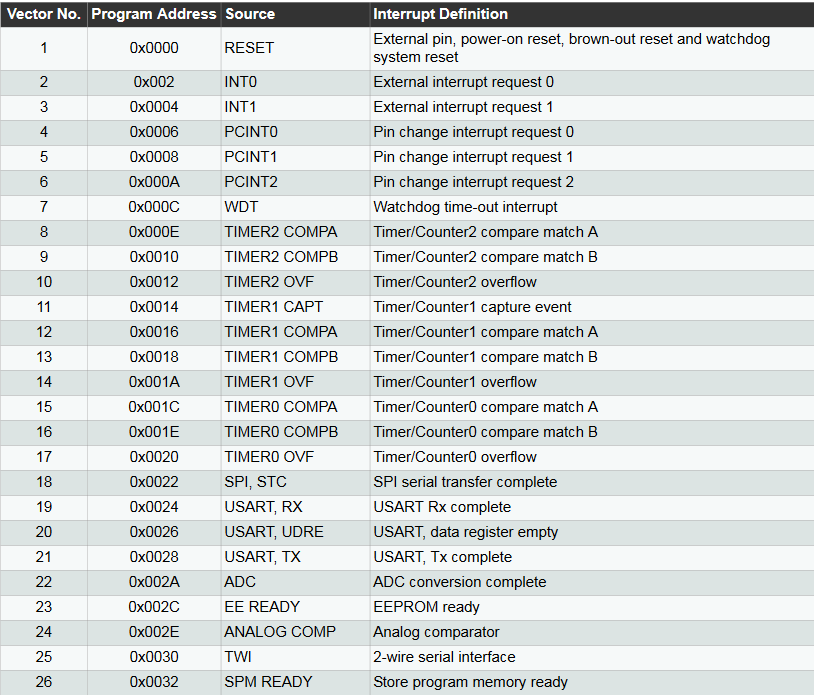
The Interrupt Vector Table contains addresses that the program counter (PC) loads when an interrupt occurs. When an interrupt is triggered, the microcontroller executes the instruction stored at the corresponding vector address.
Important
The program addresses from 0x00 – 0x32 are used for interrupt vector addresses. Therefore, when using interrupts, the main program must be stored elsewhere to avoid conflicts.
Sources of Interrupts in the AVR
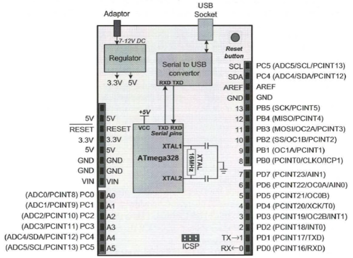
There are multiple sources of interrupts in the AVR, but we will focus on three:
- Timer-based interrupts.
- External interrupts from pins
PD2 (INT0)andPD3 (INT1) - Pin change interrupts (pins B, C, D)
Enabling the I Flag – Global Interrupt Enable
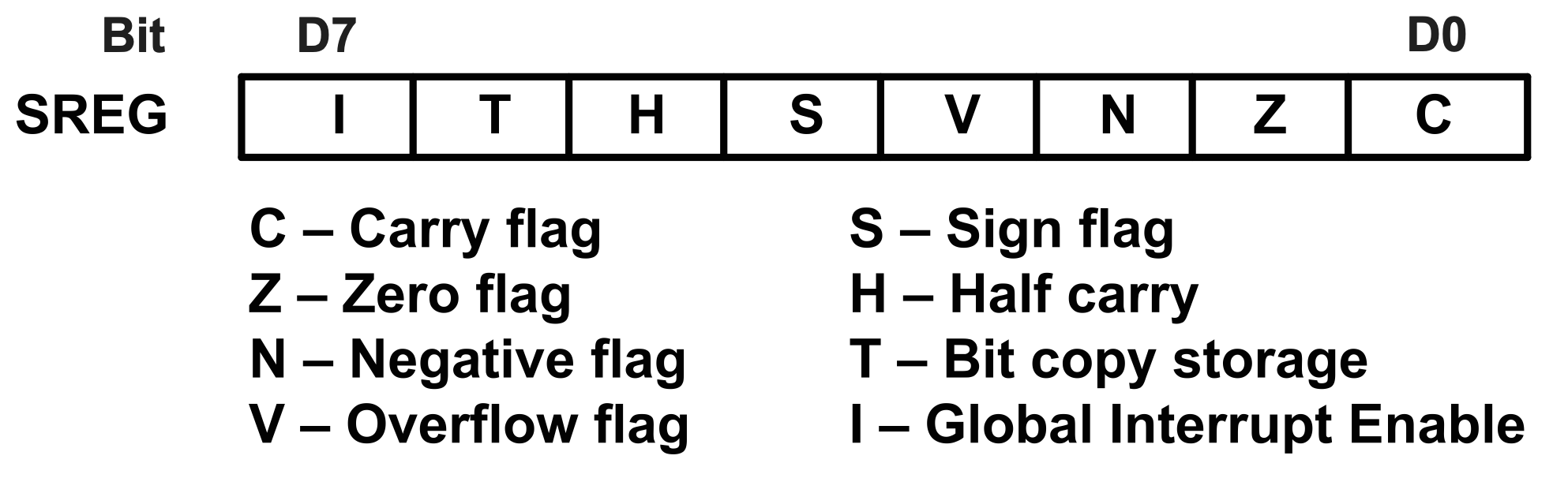
Before using an interrupt from the vector table, the global interrupt must be enabled via the I flag in the SREG register.
- Enable global interrupt: Set the I flag using
SEI(Set Interrupts). - Disable global interrupt: Clear the I flag using
CLI(Clear Interrupts). This disables all interrupts.
Programming Timer Interrupts
Timer Interrupts
Consider a scenario where a microcontroller must perform a task at a specific time (e.g., turn on an LED after 10 seconds).
- Polling Approach: Uses
SBIS TIFR0, TOV0to continuously check the TOV0 flag, preventing other tasks from running.- Will keep looking at the TOV0 flag and cannot do any thing else.
- Interrupt Approach: When the TOV0 flag is set, the microcontroller jumps to the ISR, executes it, and then resumes its previous task (when finish ISR task).
Interrupts from Timer0
The ATmega328 has three timers: Timer0, Timer1, and Timer2. We focus on Timer0, which generates three types of interrupts:
- Timer0 Overflow Interrupt (Normal Mode) →
TOIE0flag. - Timer0 Compare A Match Interrupt (CTC Mode) →
OCIE0Aflag. - Timer0 Compare B Match Interrupt (CTC Mode) →
OCIE0Bflag.
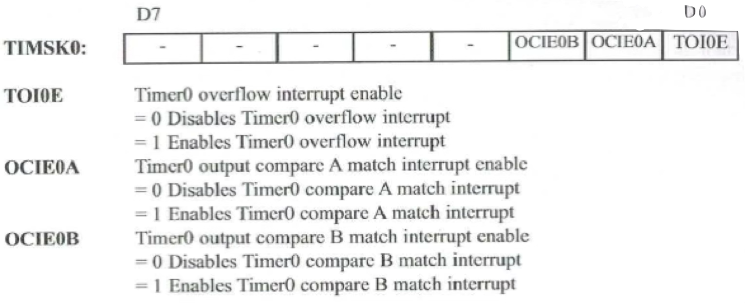
คือ Flag พวกนี้เราไม่ได้เอาไว้ใช้ Configure อะไร แต่แค่เป็นตัวบอกว่ามันล้นแล้วนะ ถึงจะ Interrupt ไป run อย่างอื่นได้???? มั่วป้ะเนี่ย
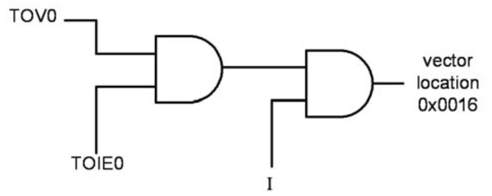
1. Timer0 Overflow Interrupt
- The
TOV0flag sets an interrupt signal to the CPU. - The CPU executes the instruction at program address
0x0020. - The instruction at
0x0020points to the ISR. - The
TOV0flag is automatically cleared when the CPU jumps to the interrupt vector table.
Steps to Use Timer0 Overflow Interrupt
- Define the interrupt vector table
- Reset interrupt (program address
0x0000). - Timer0 overflow interrupt (program address
0x0020).
- Write the main program (starting at
0x0033or later)
- Initialize the stack pointer.
- Enable Timer0 overflow interrupt using:
LDI R20, (1<<TOIE0)
STS TIMSK0, R20 - Enable global interrupt (
SEI). - Set
TCNT0and configure Timer0 mode. - Execute main tasks.
- Write the ISR (Interrupt Service Routine)
- Handles the Timer0 overflow interrupt.
- Ends with
RETIto return from the interrupt.
Example: Timer0 Overflow Interrupt
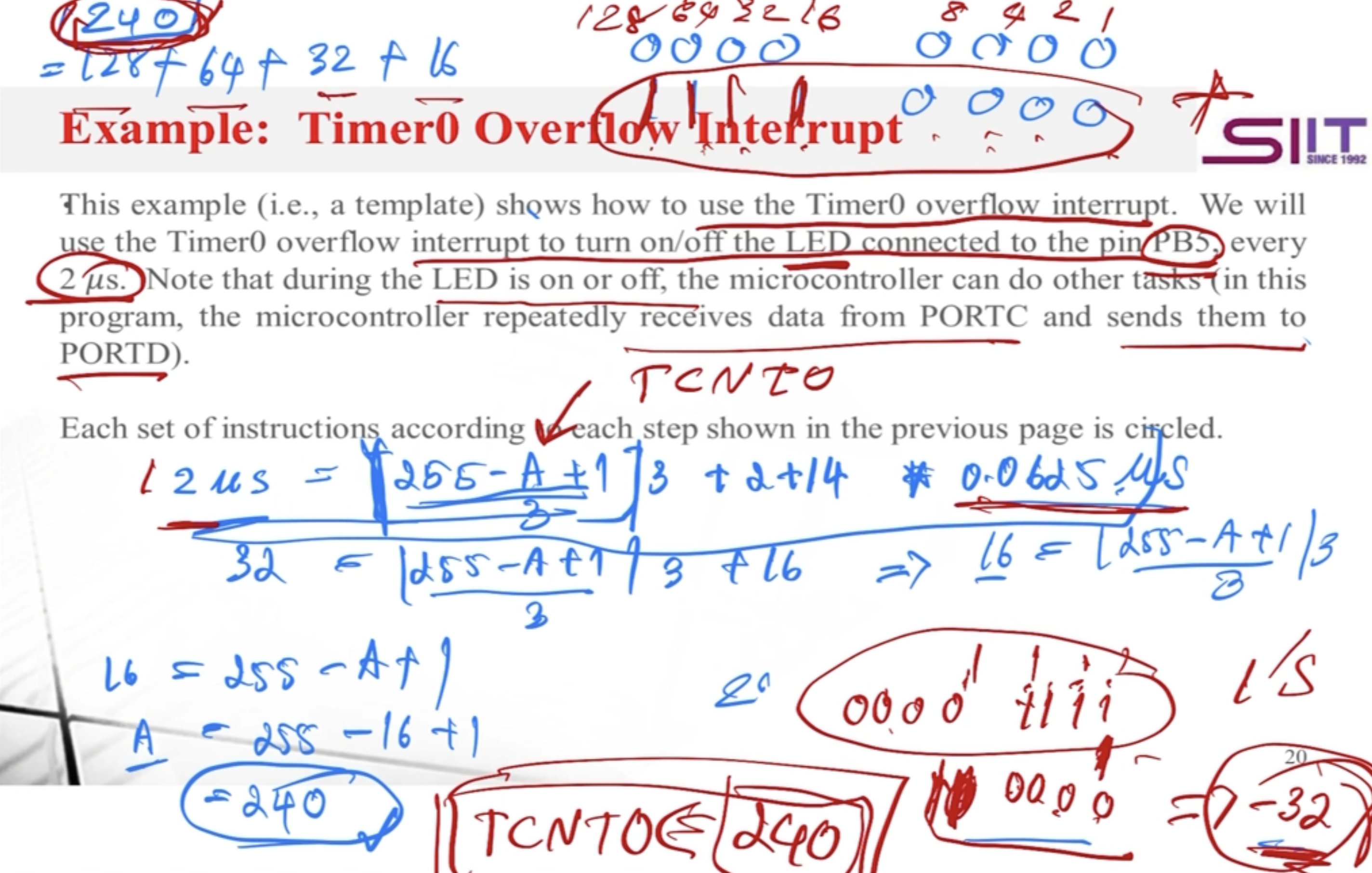
This example toggles an LED connected to PB5 every 2 µs using a Timer0 overflow interrupt. Meanwhile, the microcontroller performs other tasks (e.g., reading data from PORTC and sending it to PORTD).
.ORG 0x0
	JMP MAIN
.ORG 0x20
	JMP T0_OV_ISR

.ORG 0x100
MAIN:   LDI R20, HIGH(RAMEND)
		OUT SPH, R20
		LDI R20, LOW(RAMEND)
		OUY SPL, R20
		SBI DDRB, 5
		LDI R20, (1<<TOIE0)
		STS TIMSK0, R20
		SET

		LDI R20, -32
		OUT TCNT0, R20
		LDI R20, 0x00
		OUT TCCR0A, R20
		LDI R20, 0x01
		OUT TCCR0B, R20
		LDI R20, 0x00
		OUT DDRC, R20
		LDI R20, 0xFF
		OUT PORTC, R20
		OUT DDRD, R20
;----------- Infinite loop
HERE:   IN R20, PINC
		OUT PORTD, R20
		JMP HERE

.ORG 0x200
T0_OV_ISR:
		IN R16, PORTB
		LDI R17, (1<<5)
		EOR R16, R17
		OUT PORTB, R16
		LDI R16, -32
		OUT TCNT0, R16
		RETI ; return from interrupt
#FinalExam
📄 Lab 7 - 01 Interrupt (Timer Overflow).pdf
2. Timer0 Output CTC Interrupt
- Timer0 can generate an interrupt using CTC mode. There are two types:
- Timer0 output compare A match interrupt (used in this case).
- Timer0 output compare B match interrupt.
Operation of Output Compare A Match Interrupt
- An interrupt signal is sent when the OCF0A flag is set (
=1). - The microcontroller jumps to the program address 0x001C (ISR vector address).
- The instruction at 0x001C points to the ISR address.
- The OCF0A flag is cleared (
=0) automatically when jumping to the ISR.
Steps to Use Output Compare A Match Interrupt
- Define the Interrupt Vector Table
- Reset interrupt (program address 0x0000).
- Timer0 output compare A match interrupt (program address 0x001C).
- Main Program Initialization (starting at address >0x0033)
- Initialize stack pointer.
- Enable output compare A match interrupt:
LDI R20, (1<<OCIE0A) STS TIMSK0, R20- Enable global interrupts:
SEI - Set TCNT0 (initial timer value) and OCR0A (max timer value).
- Set Timer0 to CTC mode and start Timer0.
- Execute main tasks.
- Interrupt Service Routine (ISR)
- Executes when an interrupt occurs.
- The ISR must end with
RETI(Return from Interrupt).
Example: Output Compare A Match Interrupt
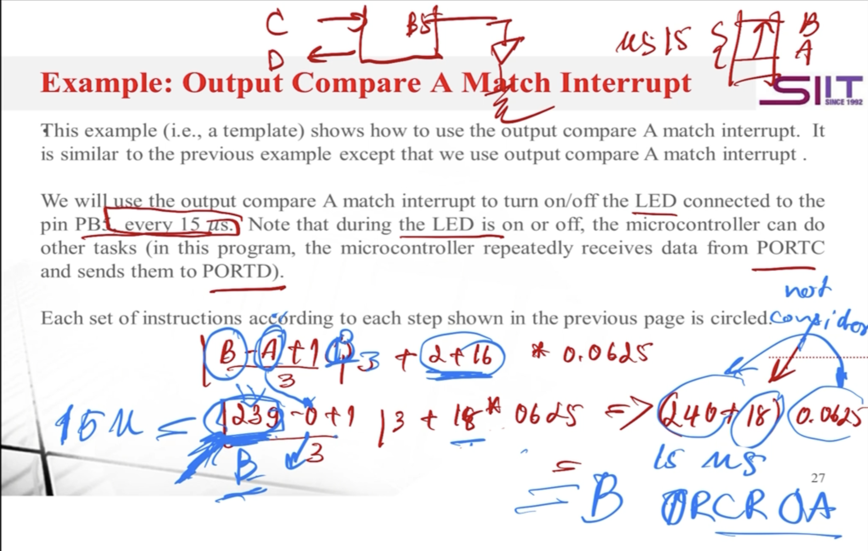
- This example demonstrates using output compare A match interrupt to toggle an LED on PB5 every 15 μs.
- During LED toggling, the microcontroller performs other tasks
- (e.g., transferring data between PORTC and PORTD).
- Each step corresponds to the structure above.
.ORG 0x0
    JMP MAIN
.ORG 0x1C ; ISR location for Timer0 compare match A
    JMP T0_CM_ISR
; Main Program Initialization
MAIN: LDI R20, HIGH(RAMEND)
      OUT SPH, R20
      LDI R20, LOW(RAMEND)
      OUT SPL, R20 ; Set up stack
      SBI DDRB, 5  ; PB5 as output

      LDI R20, 239
      OUT OCR0A, R20 ; Load Timer0 with 239
      LDI R20,(1<<WGM01)
      OUT TCCR0A, R20
      LDI R20, 0x01
      OUT TCCR0B, R20 ; Start Timer0, CTC mode, no prescaler

      LDI R20,(1<<OCIE0A)
      STS TIMSK0, R20 ; Enable Timer0 compare match interrupt
      SEI ; Enable global interrupts

      LDI R20, 0x00
      OUT DDRC, R20 ; Set PORTC as input
      LDI R20, 0xFF
      OUT DDRD, R20 ; Set PORTD as output
; Infinite Loop
HERE: IN R20, PINC ; Read from PORTC
      OUT PORTD, R20 ; Send to PORTD
      JMP HERE
; ISR for Timer0 (Executed every 40 μs)
T0_CM_ISR:
      IN R16, PORTB ; Read PORTB
      LDI R17, 1<<5 ; 00100000 to toggle PB5
      EOR R16, R17
      OUT PORTB, R16 ; Toggle PB5
      RETI ; Return from interrupt
Timer0 Interrupt with Other Timer0 Modes
We have used Timer0 interrupts in normal mode and CTC mode. It is also possible to use interrupts with:
- Normal mode with pre-scaling frequency
- CTC mode with pre-scaling frequency
Refer to Lecture 7 for more details.
Programming External Hardware Interrupts
External Hardware Interrupts
ATmega328 has two external hardware interrupts: INT0 and INT1.
- INT0 (External Interrupt 0) is triggered by a signal change on PD2.
- When a signal change happens at the pin PD2, the INT0 interrupt occurs.
- When triggered, the microcontroller jumps to program address 0x0002.
- This address points to the ISR.
- INT1 (External Interrupt 1) is triggered by a signal change on PD3.
- When a signal change happens at the pin PD3, the INT1 interrupt occurs.
- When triggered, the microcontroller jumps to program address 0x0004.
- This address points to the ISR.
Registers and Flags Related to the External INT0/INT1 Interrupts
Two key registers control external interrupts:
- EIMSK (External Interrupt Mask Register)
- Contains flags to enable INT0 and INT1.
- EICRA (External Interrupt Control Register A)
- Contains the ISC00, ISC01, ISC10, and ISC11 flags.
- Controls how the interrupts are triggered (low-level, edge-triggered, etc.).
The EIMSK Register
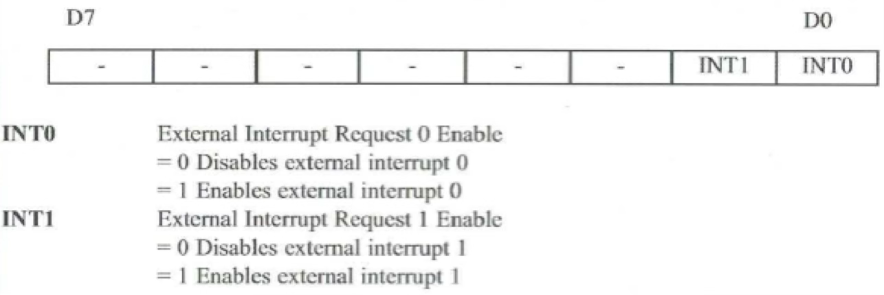
Contains two flags for enabling external interrupts:
- INT0 (bit 0): Enables INT0 interrupt (PD2).
- This flag must be set to enable the INT0 interrupt (from the pin PD2)
LDI R20, (1<<INT0) OUT EIMSK, R20 SEI - INT1 (bit 1): Enables INT1 interrupt (PD3).
- This flag must be set to enable the INT1 interrupt (from the pin PD3)
LDI R20, (1<<INT1)
OUT EIMSK, R20
SEI
The EICRA Register
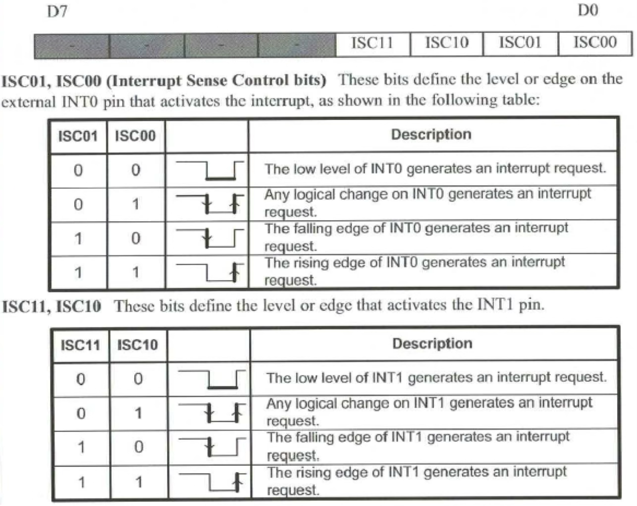
The EICRA register controls when the INT0/INT1 interrupts are triggered.
- ISC01, ISC00: Set INT0 conditions.
- ISC11, ISC10: Set INT1 conditions.
By default (all bits = 0), INT0/INT1 are low-level triggered.
Setting INT0 Conditions
Note that the STS instruction is used instead of the OUT instruction.
- Low-level triggering (default):
- Change-level triggering:
LDI R20, (1<<ISC00) STS EICRA, R20 - Falling-edge triggering:
LDI R20, (1<<ISC01) STS EICRA, R20 - Rising-edge triggering:
LDI R20, (1<<ISC01)|(1<<ISC00)
STS EICRA, R20
Setting INT1 Conditions
(Similar to INT0 but using ISC11, ISC10) — เหมือนกันเลยนะ 00 → 10, 01 → 11 แค่นั้น!
Remarks
- Edge-triggered conditions (change, falling, rising) require at least 1 instruction cycle for proper detection.
- Level-triggered condition (input PD2, PD3 must be low) requires at least 5 instruction cycles for stability.
Using the INT0 Interrupt
- To set up INT0, follow these steps:
- (Note that using the INT1 interrupt can be set up in a similar way.)
- Define interrupt vector table.
- Reset interrupt ()
- INT0 interrupt ()
- Main program setup (Starts at > 0x0033):
- Initialize stack pointer.
- Enable pull-up resistor on PD2.
- Configure EICRA for INT0 condition. (ISC00, ISC01)
- Enable EIMSK and global interrupt flag.
- Execute main tasks.
- Define Interrupt Service Routine (ISR) at 0x0002. (0x0002 นี่จริงมั้ย เช็คอีกที)
- ISR executes on INT0 interrupt.
- Ends with
RETIinstruction.
Example: INT0 Interrupt
The program toggles PB5 when INT0 is triggered (PD2 goes HIGH → LOW).
.ORG 0 ; Reset location
    JMP MAIN
.ORG 0x02 ; INT0 interrupt vector
    JMP EX0_ISR

MAIN:
    LDI R20, HIGH(RAMEND)
    OUT SPH, R20
    LDI R20, LOW(RAMEND)
    OUT SPL, R20 ; Initialize stack

    LDI R20, 0x2 ; Falling-edge trigger (ISC01=1, ISC00=0)
    STS EICRA, R20
    SBI DDRB, 5 ; Set PB5 as output
    SBI PORTD, 2 ; Enable pull-up on PD2
    LDI R20, 1<<INT0 ; Enable INT0
    OUT EIMSK, R20
    SEI ; Enable global interrupts

HERE: JMP HERE

EX0_ISR:
    IN R21, PORTB
    LDI R22, (1<<5) ; Toggle PB5
    EOR R21, R22
    OUT PORTB, R21
    RETI
This example keeps the microcontroller busy in a HERE loop while waiting for interrupts. When INT0 occurs, PB5 toggles state.
📄 Lab 7 - 02 Interrupt (External).pdf
Programming Pin Change Interrupts
Pin Change Interrupts
- In ATmega328, a pin change interrupt is triggered when an input signal changes at an I/O pin (PORT B, C, or D).
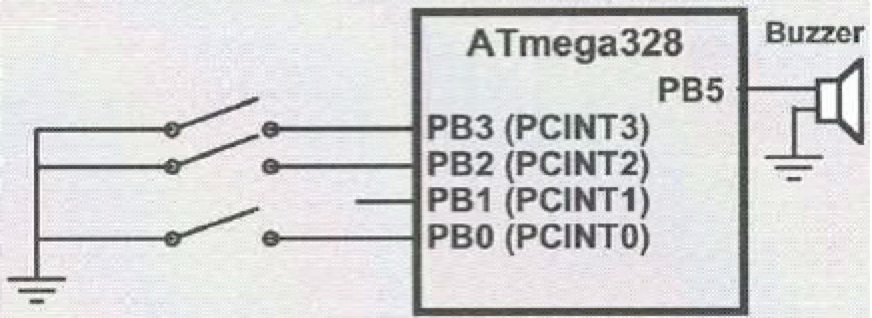
- Two registers are needed to configure a pin change interrupt:
- PCICR (Pin Change Interrupt Control Register)
- PCMSK (Pin Change Mask Register)
Register: PCICR
- The PCICR register consists of three flags: PCIE0, PCIE1, and PCIE2, each enabling pin change interrupts for PORT B, C, and D, respectively.
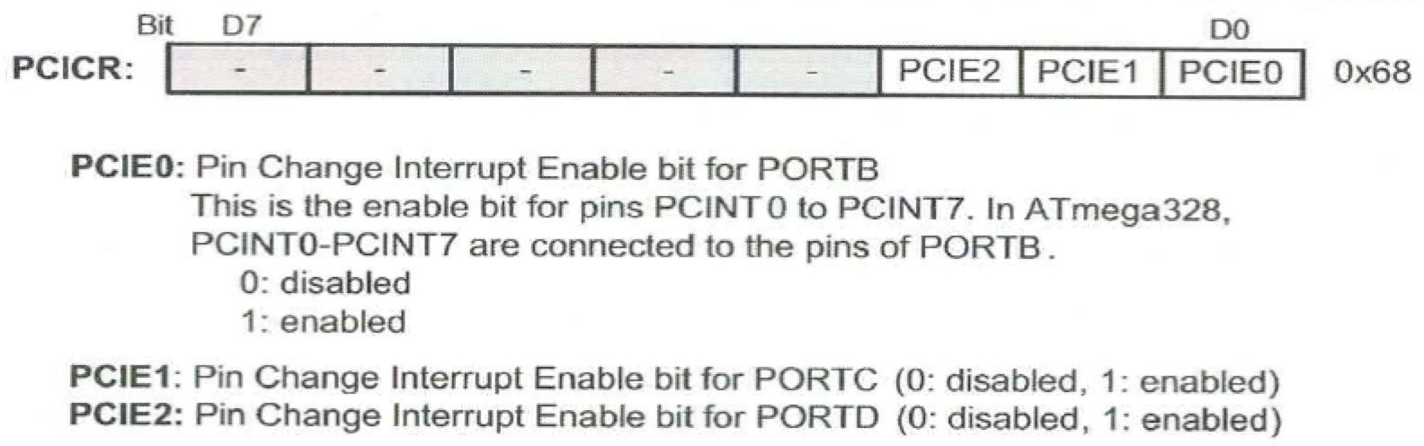
- Example: Enabling pin change interrupts for PORT B:
LDI R20, (1<<PCIE0)
STS PCICR, R20
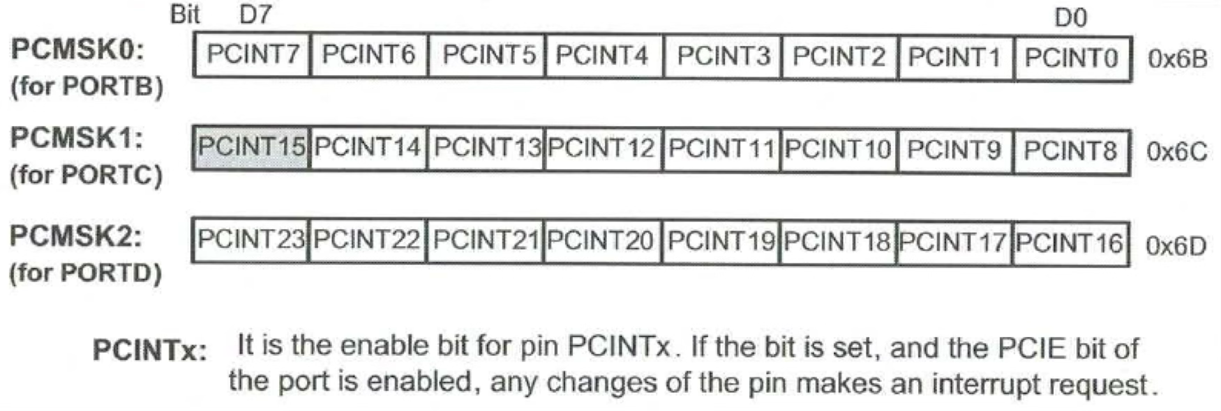
Registers: PCMSK
- Three PCMSK registers configure which pins trigger an interrupt: (each register consists of 8 bits)
- PCMSK0 (for PORT B)
- PCMSK1 (for PORT C)
- PCMSK2 (for PORT D)
- Example: Enabling pin change interrupts for PB0, PB2, and PB3:
LDI R20, 0b00001101
STS PCMSK0, R20
Interrupt Vector Table
Each PORT has a dedicated interrupt vector:
- PORT B → Address 0x0006 (the microcontroller will go to the program address 0x0006)
- PORT C → Address 0x0008
- PORT D → Address 0x000A
These addresses point to their respective Interrupt Service Routines (ISRs).
Using the Pin Change Interrupt
Steps to implement a pin change interrupt:
- Define the interrupt vector table
- Reset interrupt at 0x0000
- Pin change interrupts at 0x0006, 0x0008, or 0x000A
- Main Program (Starts at > 0x0033)
- Initialize Stack Pointer
- Set PCMSK0/1/2 (using STS, not OUT)
- These pins will be in the input mode automatically.
- Set pull-up resistors on input pins
- Enable PCIE0/1/2 in PCICR (using STS)
- Enable global interrupts using SEI
- Perform main tasks
- Interrupt Service Routine (ISR)
- Execute ISR when an interrupt occurs
- End ISR with RETI
Example: Pin Change Interrupt
Scenario: PB0, PB2, and PB3 are connected to switches. When any switch state changes, PB5 is set high.
.ORG 0 ; Reset vector
    JMP MAIN
.ORG 0x06 ; Pin Change Interrupt 0 vector
    JMP PCINT0_ISR

MAIN:
    LDI R20, HIGH(RAMEND)
    OUT SPH, R20
    LDI R20, LOW(RAMEND)
    OUT SPL, R20 ; Initialize stack

    SBI DDRB, 5 ; PB5 as output
    CBI PORTB, 5 ; PB5 = low
    LDI R20, 0b00001101
    STS PCMSK0, R20 ; Enable PB0, PB2, PB3 in PCMSK0
    OUT PORTB, R20 ; Enable pull-ups
    LDI R20, (1<<PCIE0)
    STS PCICR, R20 ; Enable PORTB change interrupt
    SEI ; Enable global interrupts

HERE:
    JMP HERE ; Infinite loop

PCINT0_ISR:
    SBI PORTB, 5 ; PB5 = high
    RETI ; Return from interrupt
This example configures pin change interrupts and demonstrates a simple ISR execution.