#Summarized
How to config microcontroller when we want to use timer/counter of that microcontroller.
AVR Timer/Counter Structure
Introduction: On/Off an LED Every 2 Seconds
- A common method for creating a time delay in microcontrollers is using nested loops with register decrements. However, a more efficient way is using hardware timers.
Example: LED Blinking with Delay
The following assembly code toggles an LED every 2 seconds using a software delay subroutine (DELAY).
	.ORG 0  ; Origin of the program in memory

	; Stack Initialization (used for function calls)
	LDI R16, HIGH(RAMEND) ; Load the high byte of the RAM end address into R16
	OUT SPH, R16          ; Set the Stack Pointer High (SPH)
	LDI R16, LOW(RAMEND)  ; Load the low byte of the RAM end address into R16
	OUT SPL, R16          ; Set the Stack Pointer Low (SPL)

	; Pin Configuration
	SBI DDRD, 4           ; pinMode(4, OUTPUT);
	CBI PORTD, 4          ; digitalWrite(4, LOW);
	SBI DDRD, 5           ; pinMode(5, OUTPUT);
	CBI PORTD, 5          ; digitalWrite(5, LOW);

AGAIN:
	SBI PORTD, 4      ; digitalWrite(4, HIGH);
	CBI PORTD, 5      ; digitalWrite(5, LOW);
	CALL DELAY        ; Call the delay subroutine
	CBI PORTD, 4      ; digitalWrite(4, LOW);
	SBI PORTD, 5      ; digitalWrite(5, HIGH);
	CALL DELAY        ; Call the delay subroutine
	RJMP AGAIN        ; Repeat loop

DELAY:  ; Delay subroutine
	LDI R20, 128
L1:	LDI R21, 200
L2:	LDI R22, 250
L3:	NOP
	NOP
	DEC R22
	BRNE L3
	DEC R21
	BRNE L2
	DEC R20
	BRNE L1
	RET
This is the traditional method. Let's explore using timers instead!
Basic Idea of Timers/Counters
- A microcontroller has a hardware timer/counter module that counts clock pulses. It serves two purposes:
- Timer Mode – Creates a time delay based on an internal clock.
- Counter Mode – Counts external events from an external clock signal.
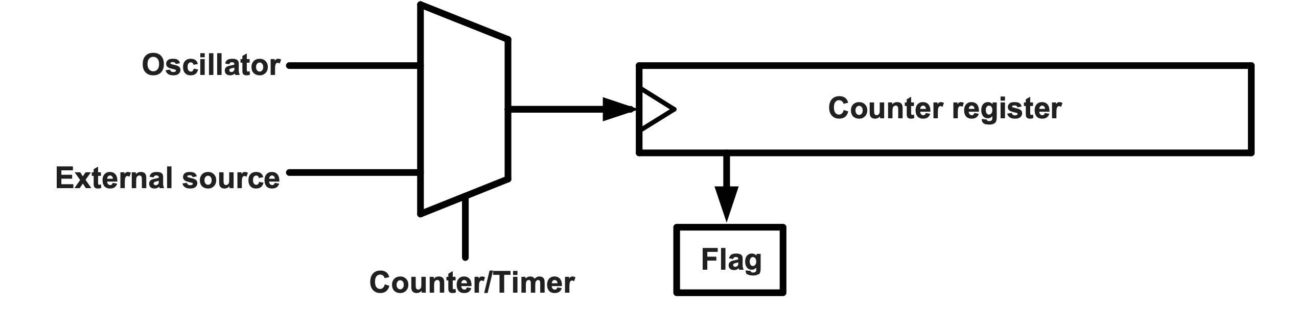
Basic Components of Timers/Counters
- Inputs to Timer/Counter
- Internal Clock Source (e.g., 16MHz quartz crystal oscillator)
- Used for both instruction execution and timer operations.
- External Clock Source (e.g., square wave input to a timer pin like
T0).
- Internal Clock Source (e.g., 16MHz quartz crystal oscillator)
- Timer/Counter Circuit
- Detects rising or falling edges of clock pulses.
- Counter Register
- Stores the number of counted clock pulses.
- Example: An 8-bit register can count from
0x00to0xFF(0–255).
- Flag Bit
- A 1-bit flag is set when the counter reaches a predefined value.
Timer vs. Counter
| Mode | Input Source | Usage |
|---|---|---|
| Timer | Internal clock (e.g., 16MHz) | Time delay |
| Counter | External clock (e.g., function generator) | Event counting |
| For now, we will focus on timers only. |
ATmega328 Timers
The ATmega328 (used in Arduino Uno) has 3 timers:
- Timer0 → 8-bit counter ✅ (Covered here)
- Timer1 → 16-bit counter
- Timer2 → 8-bit counter
Next, we’ll explore how to configure Timer0 for precise time delays. 🚀
Timer0: Timer Structure
A diagram of the Timer0 hardware structure is shown below:
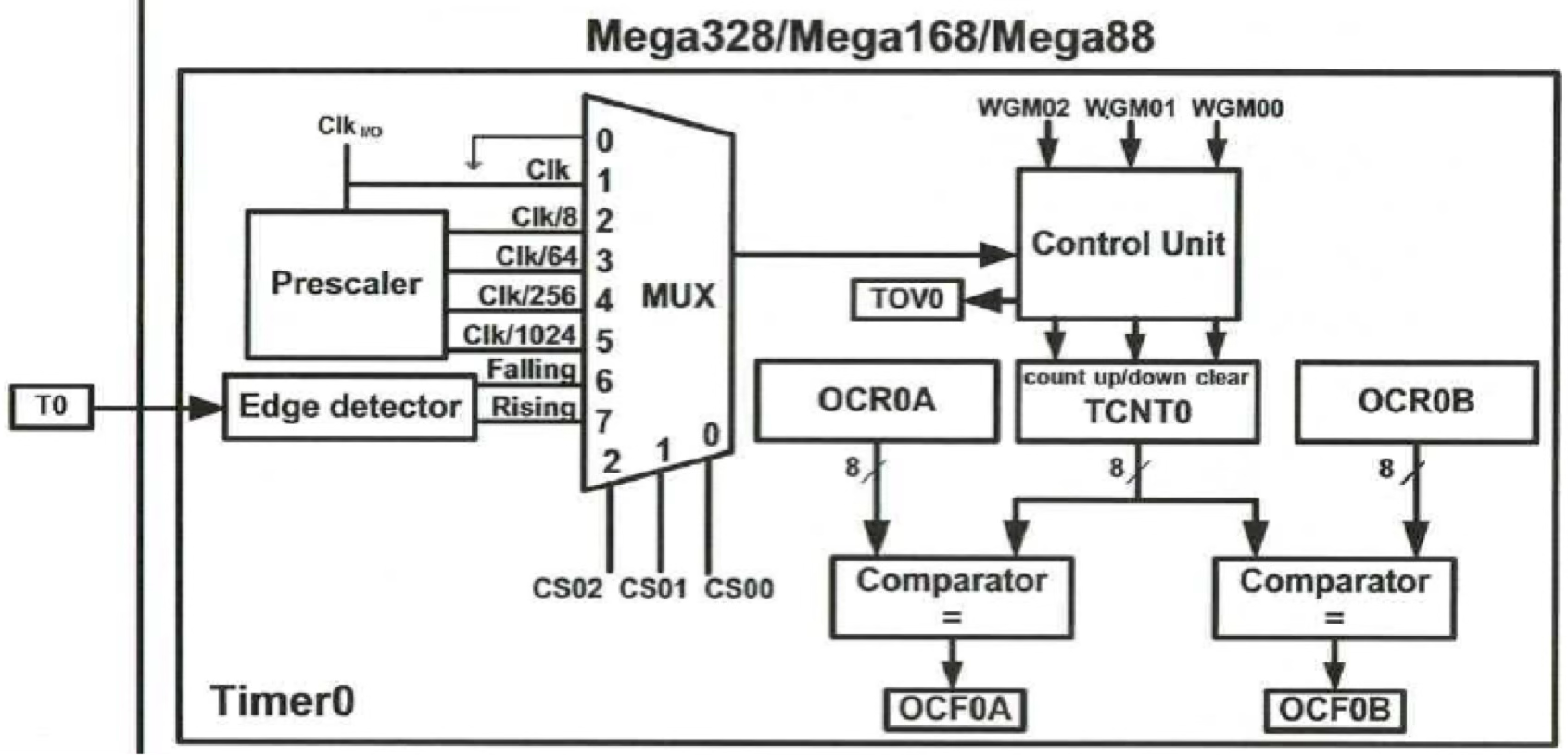
- Input Source
Clk→ Internal clock (16MHz crystal oscillator).T0→ External clock input via PD4 pin.
- Edge Detector
- Detects rising or falling edge of the external clock.
- MUX (Multiplexer)
- Selects the clock input based on flags
CS02,CS01,CS00.
- Selects the clock input based on flags
- Control Unit
- Updates the clock pulse count.
- Uses
WGM02,WGM01,WGM00to set the timer mode. TOV0(Timer Overflow Flag) is set when TCNT0 overflows (0xFF → 0x00).
- TCNT0 Register
- Stores the current clock pulse count.
- 8-bit register (
0x00 – 0xFF).
- OCR0A & OCR0B Registers
- Store the target pulse count for comparison. (Store number of clock pulse we want!)
- OCF0A & OCF0B Flags
- Set to
1whenTCNT0 == OCR0AorTCNT0 == OCR0B.
- Set to
Timer0: Registers and Flags
TCNT0 register
- Stands for Timer/Counter 0.
- 8-bit register (memory address
0x46). - Stores the current pulse count and increments with each clock tick!
- We can set it to start at any number between 0x00 – 0xFF.
- When TCNT0 overflows (
0xFF → 0x00), TOV0 flag is set.

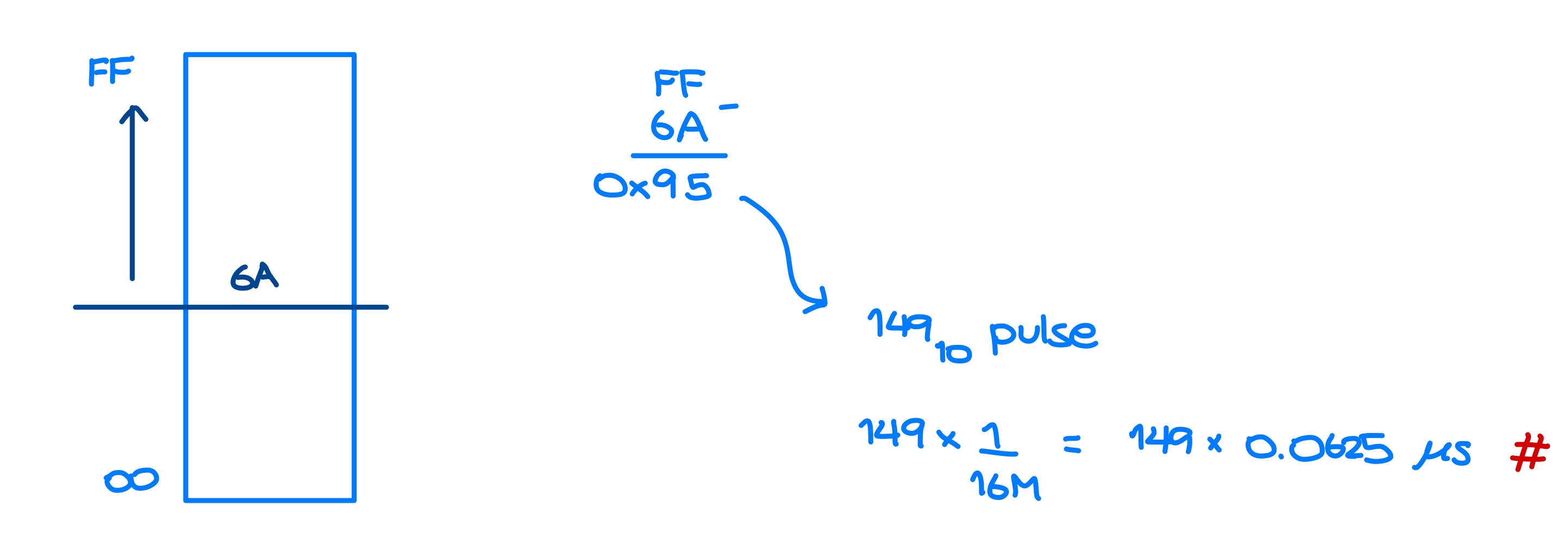
Example Calculation
Given:
- Initial TCNT0 = 0x00
- Current TCNT0 = 0x6A
- Clock frequency = 16MHz
How many clock pulses have passed?
How much time has elapsed?
TCCR0A and TCCR0B Registers
TCCR0A(Timer/Counter Control Register A)- 8-bit register, memory address:
0x44.
- 8-bit register, memory address:
TCCR0B(Timer/Counter Control Register B)- 8-bit register, memory address:
0x45.
- 8-bit register, memory address:
- These registers are used to configure Timer0:
- Operation mode (Normal, CTC, etc.)
- Input source (Internal/external clock)
- The structure of the TCCR0A register is shown below.

- The structure of the TCCR0B register is shown below.

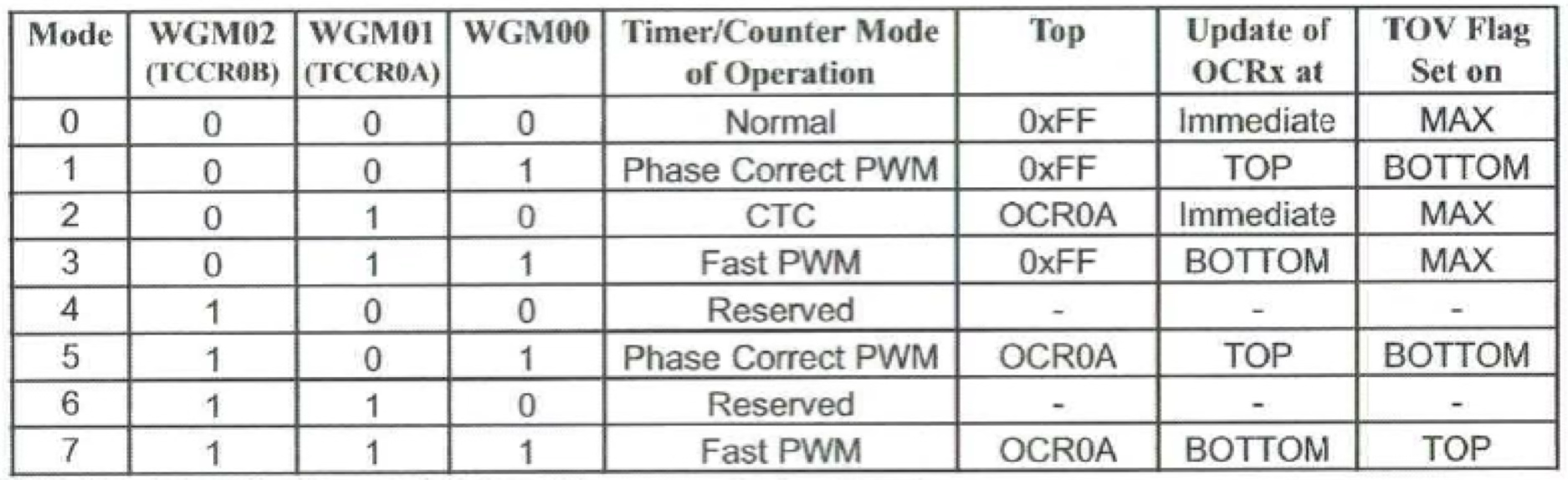
Timer Operation Modes (Selected via WGM02, WGM01, WGM00)
Timer operation mode. There are 8 timer operation modes. We use the flags WGM02, WGM01, WGM00 to set the Timer0 operation mode. Two modes will be studied here.
| Mode | WGM02 | WGM01 | WGM00 | Description |
|---|---|---|---|---|
| Normal | 0 | 0 | 0 | Counts to 0xFF, then resets to 0x00 (TOV0 flag set). |
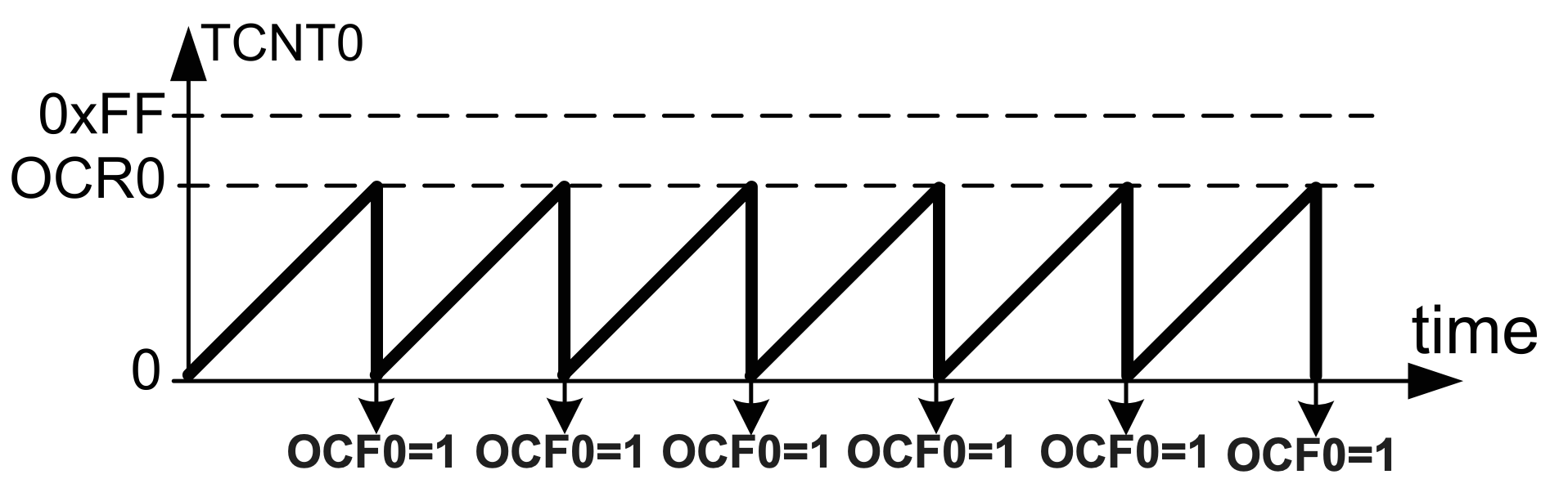
| CTC (Clear Timer on Compare Match) | 0 | 1 | 0 | Counts to OCR0A value, then resets to 0x00 (OCF0A flag set). ไปจนถึงตัวเลขที่เรากำหนดไว้ |
| Other modes | - | - | - | Not covered here. |
- The other modes are shown in the next table. (แต่เราจะสนใจแค่ Normal, CTC)
Example: Configure Timer0 for Normal Mode
; Set Normal mode
LDI R16, 0x00
OUT TCCR0A, R16
Timer Input Source (Selected via CS02, CS01, CS00)
| CS02:00 | Input Clock Source |
|---|---|
000 | No clock (Timer stopped) |
001 - 101 | Internal clock (with/without prescaling) |
110 - 111 | External clock |
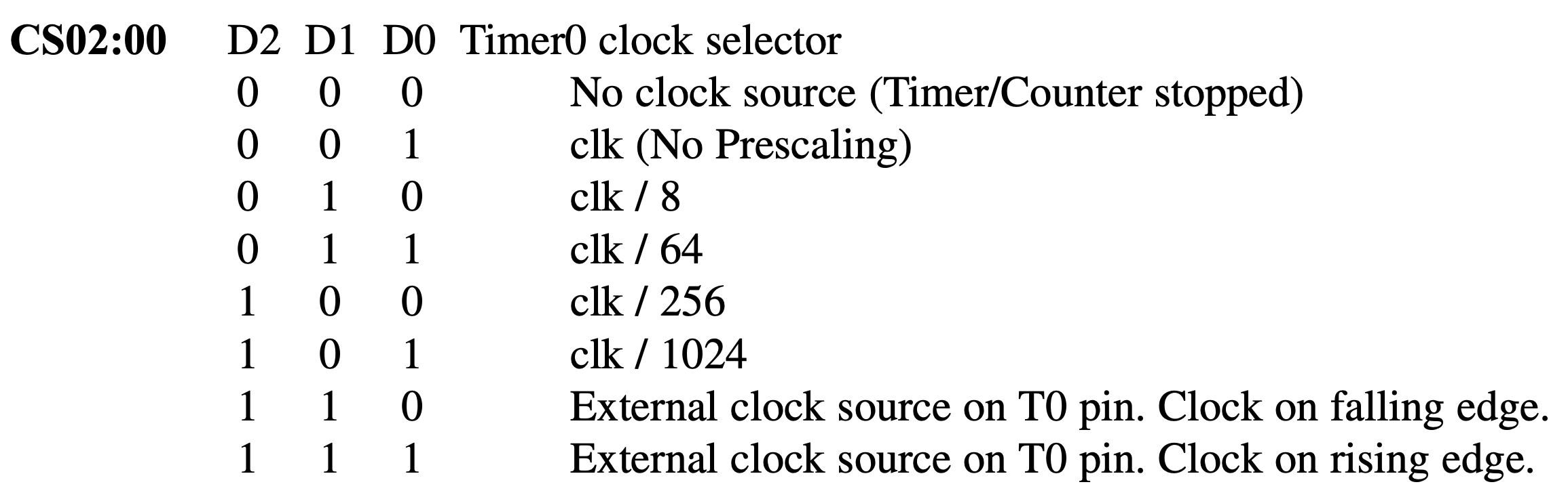 |
Example: Configure Timer0 with Internal Clock (No Prescaler)
Write an Assembly program to set Timer0 to work as follows.
; No prescale (use original clock frequency)
LDI R16, 0x01
OUT TCCR0B, R16
OCR0A and OCR0B Registers
- OCR0A (Output Compare Register A)
- Stores an 8-bit value that is compared with TCNT0.
- When
TCNT0 == OCR0A, OCF0A flag is set (=1). - Memory address:
0x47.
- OCR0B (Output Compare Register B)
- Similar to
OCR0A, but with its own compare flag (OCF0B). - Memory address:
0x48.
- Similar to
- We will use the OCR0A register in the CTC operation mode.
Example: Store 0xAA in OCR0A
LDI R16, 0xAA
OUT OCR0A, R16
TIFR0 Register (Timer/Counter Interrupt Flag Register 0)
- Memory address:
0x35. - Contains flags that indicate timer events:
- TOV0 → Set (
=1) whenTCNT0overflows (0xFF → 0x00). - OCF0A → Set (
=1) whenTCNT0 == OCR0A. - OCF0B → Set (
=1) whenTCNT0 == OCR0B.
- TOV0 → Set (
ก็คือถ้าใช้ Normal Mode จะเป็น
SBIS TIFR0, 0
แต่ถ้าเป็น CTC Mode จะเป็นSBIS TIFR0, 1
- Its structure is shown below.

Using Timer0 as a Timer
In this section, we will set up and use Timer0 as a timer (i.e., internal clock input). The following three modes are studied:
- Normal Mode (No Pre-Scaling Frequency)
- Normal Mode (With Pre-Scaling Frequency)
- CTC (Compare Match) Mode
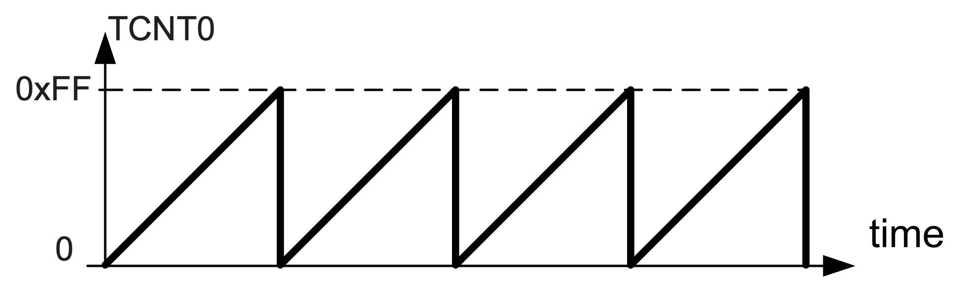
Normal Mode (No Pre-Scaling Frequency)
In this mode, Timer0 operates with the following specifications:
- Clock source: Internal 16 MHz crystal clock (ATmega328P)
- Counting range:
0x00to0xFF(255) - Overflow behavior: When
TCNT0rolls over from0xFF → 0x00,TOV0flag is set (=1).
The operation of Normal Mode can be visualized below:
Steps to Generate a Time Delay Using Timer0
- Load
TCNT0register with an initial value. - Set
TCCR0AandTCCR0Bregisters as follows:CS02:CS00 = 001→ No pre-scalingWGM02:WGM00 = 000→ Normal mode- Other flags =
0 - This results in:
TCCR0A = 0b00000000 = 0x00TCCR0B = 0b00000001 = 0x01(starts the timer)
- Monitor
TOV0flag and exit the loop whenTOV0 = 1. - Stop Timer0 by setting
TCCR0B = 0x00.- มันก็ต้อง
LDIValue เข้ามาก่อน แล้วค่อย Set ให้มันนะ!
- มันก็ต้อง
- Clear
TOV0flag for the next round.- To clear an AVR flag, write
1to it:LDI R20, 0x01 OUT TIFR0, R20 ; Clear TOV0
- To clear an AVR flag, write
- Repeat Step 1 for continuous operation.
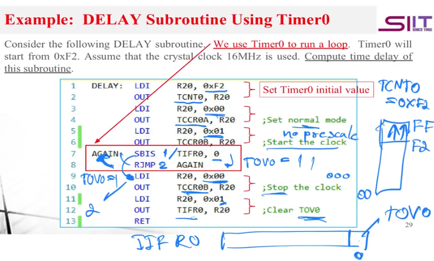
Example: DELAY Subroutine Using Timer0
Consider the DELAY subroutine using Timer0, which starts from 0xF2.
Solution
Timer0runs in theAGAINloop.- The
SBIS TIFR0, 0instruction checksTOV0:- If
TOV0 = 1, exit the loop. - If
TOV0 = 0, stay in the loop.
- If
- Loop execution analysis:
SBIStakes 1 or 2 cycles (depending on condition).RJMPtakes 2 cycles.- Each loop iteration requires 3 cycles.
- TCNT0 Increments:
0xF2 → 0xF5 → 0xF8 → 0xFB → 0xFE → 0x01 (overflow, TOV0 is set)- Repeats 5 times before
TOV0is set. - Exiting loop takes 2 cycles.
- Repeats 5 times before
- Total cycles in loop:
- Total instruction cycles for DELAY subroutine:
- Time delay calculation:
where
0.0625 µsis the period of a 16 MHz clock.
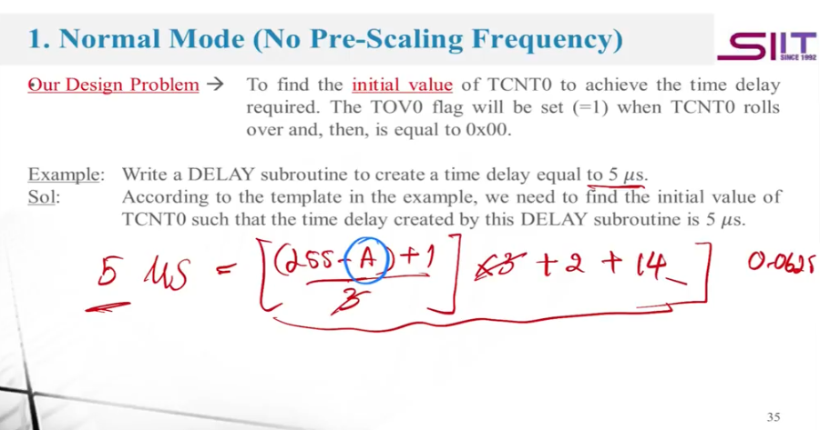
General Formula for Time Delay Calculation
From the previous example, the time delay formula for a DELAY subroutine using Timer0 is:
where:
- = Initial value of
TCNT0 - =
0xFF(maximum count) - = Ceiling operator
Design Problem:
Normal Mode with a Pre-Scaling Frequency
If we need a larger time delay, we can set Timer0 to work with a pre-scaled clock to slow down the timer increments. The available pre-scaling options are:
| Pre-Scaling Factor | Effect |
|---|---|
| clk/8 | Every 8 clock cycles → TCNT0 increments by 1 |
| clk/64 | Every 64 clock cycles → TCNT0 increments by 1 |
| clk/256 | Every 256 clock cycles → TCNT0 increments by 1 |
| clk/1024 | Every 1024 clock cycles → TCNT0 increments by 1 |
| 
Register Configuration
- Mode Selection:
- Set
WGM02:WGM00 = 010for CTC Mode.
- Set
- Pre-Scaling Selection:
- Use
CS02:CS00to control clock speed (frequency).
- Use
Steps for a Time Delay using CTC Mode
- Set the initial value in
TCNT0. - Set the compare match value in
OCR0A(max value). - ==Configure CTC mode & pre-scaling (modify
TCCR0AandTCCR0B).== - Implement a polling loop:
- Stay in the loop while OCF0A = 0.
- Exit when OCF0A = 1.
- Stop Timer0.
- Clear OCF0A flag.
Example: CTC Mode with No Pre-Scaling (clk/1)
Problem Statement:
Compute the time delay when:
- Initial Value:
TCNT0 = 0x25 - Max Compare Value:
OCR0A = 0x5A - No pre-scaling (
clk/1)
Solution:
-
Compute Loop Iterations (
N) -
Total Cycles in Loop (
AGAIN)- Since each iteration takes 3 cycles, total cycles spent:
- Add 2 cycles for exiting the loop → 56 cycles.
-
Other Instructions:
- Additional 16 instruction cycles.
-
Total Instruction Cycles:
-
Time Delay Calculation:
- Each cycle duration = 0.0625 µs (for 16 MHz clock).
General Formula for Time Delay in CTC Mode
To calculate the time delay in CTC Mode, use:
where:
- = Initial
TCNT0value - = Max
OCR0Avalue - = Pre-scaling factor (1, 8, 64, 256, or 1024)
- = Ceiling function
บางครั้งก็ถาม A (ให้ B มา) ต้องให้อย่างใดอย่างนึงนะ!
Design Problem: Finding Timer Parameters
Given a required time delay, determine:
- Initial
TCNT0value (A) - Max
OCR0Avalue (B) - Pre-scaling factor (
P)
Key Constraint:
- OCF0A flag is set (
=1) whenTCNT0rolls overOCR0Aand resets to0x00.