I/O Pins and I/O Port Registers
I/O Pins of ATmega328
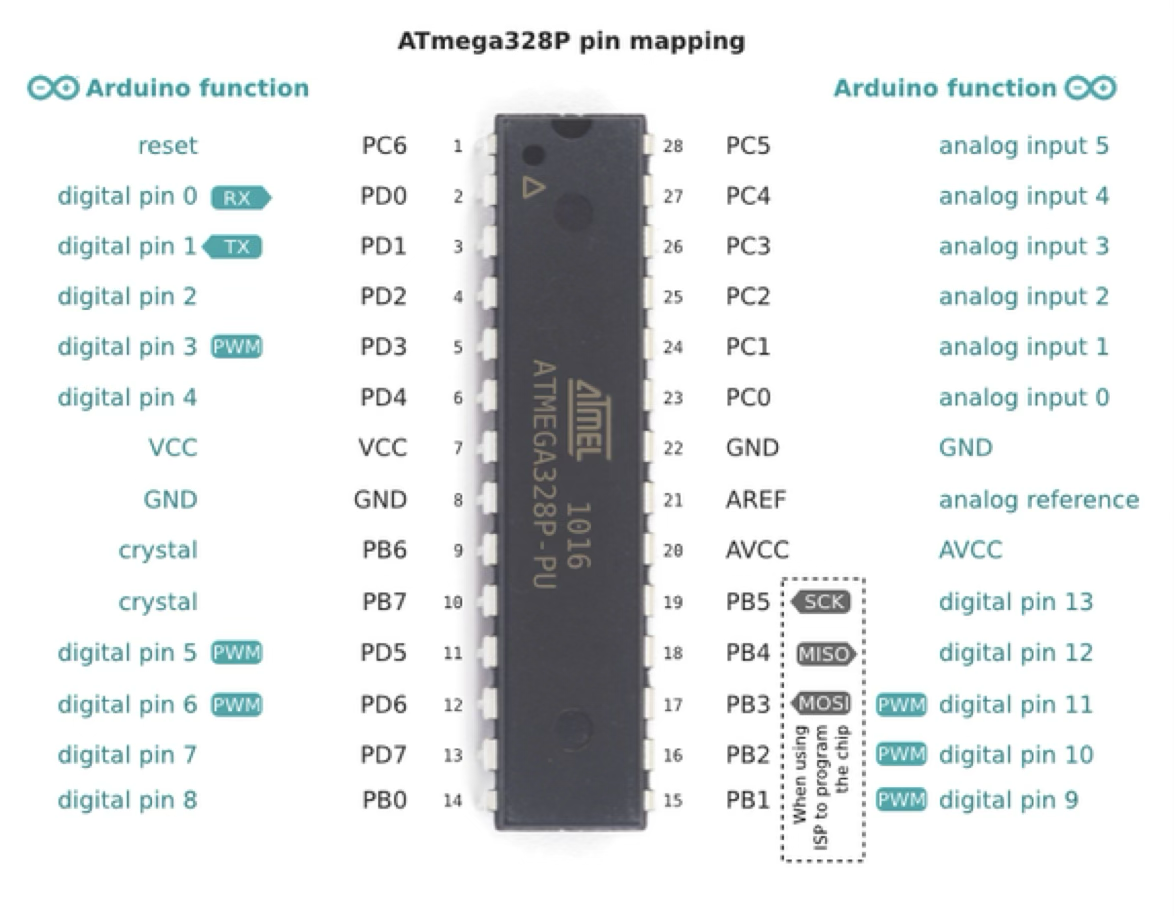
The ATmega328 has 28 pins that connect to external devices. These pins function as:
- Input pins → Read values from external devices.
- Output pins → Write values to external devices.
I/O Pin Groups:
- Port B (PB0 – PB7) → 8 pins
- Port C (PC0 – PC5) → 6 pins
- Port D (PD0 – PD7) → 8 pins
- The remaining 6 pins: VCC, GND, RESET, AREF, AGND, AVCC.
- Pins must be programmed to function as input or output.
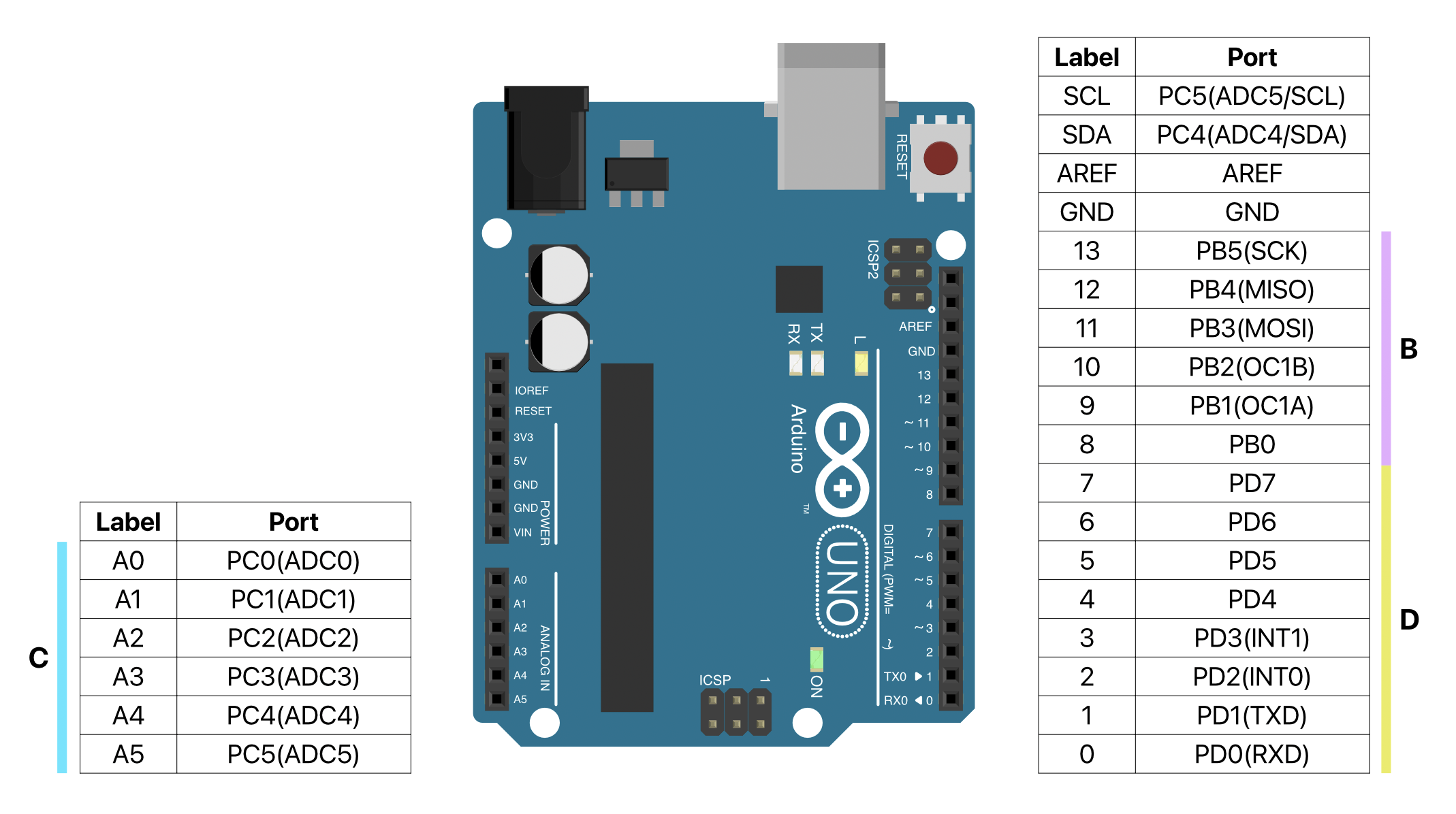
I/O Pins of Arduino UNO Board
I/O Port Registers
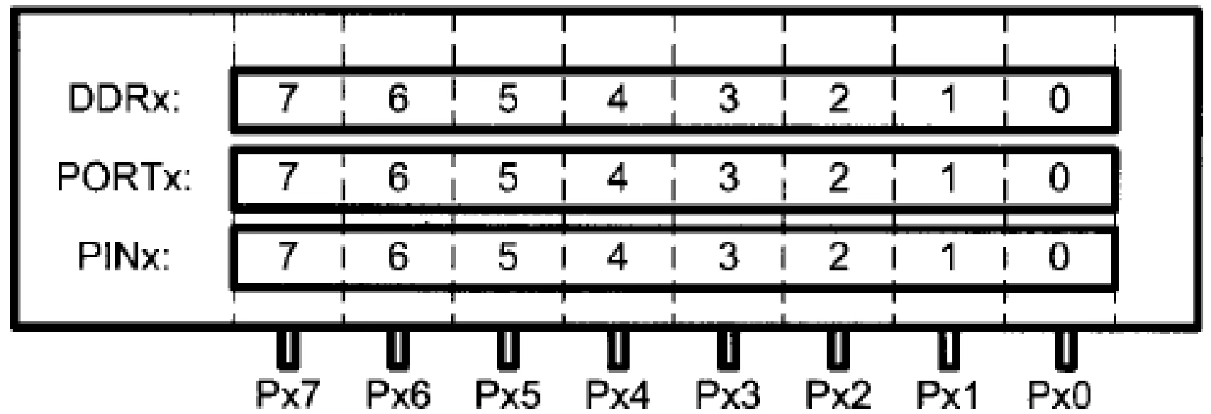
Each port (B, C, D) has 3 key registers to control pin behavior:
- DDRx → Sets the direction (input/output).
- PORTx → Sends data to output pins.
- PINx → Reads data from input pins.
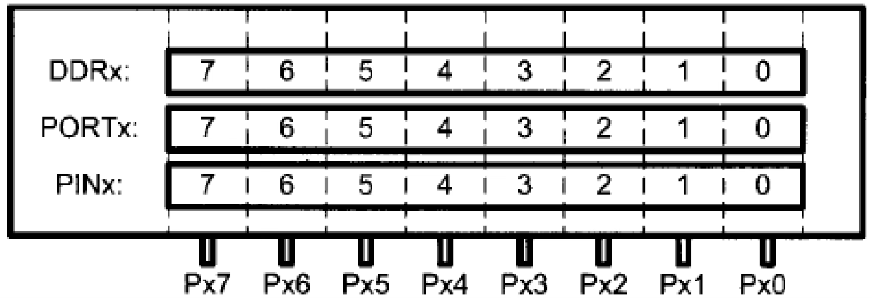
Register Functions:
- PINx Register: Stores values received from input pins.
- PORTx Register: Stores values sent to output pins.
- DDRx Register: Determines whether pins act as input (
0) or output (1).
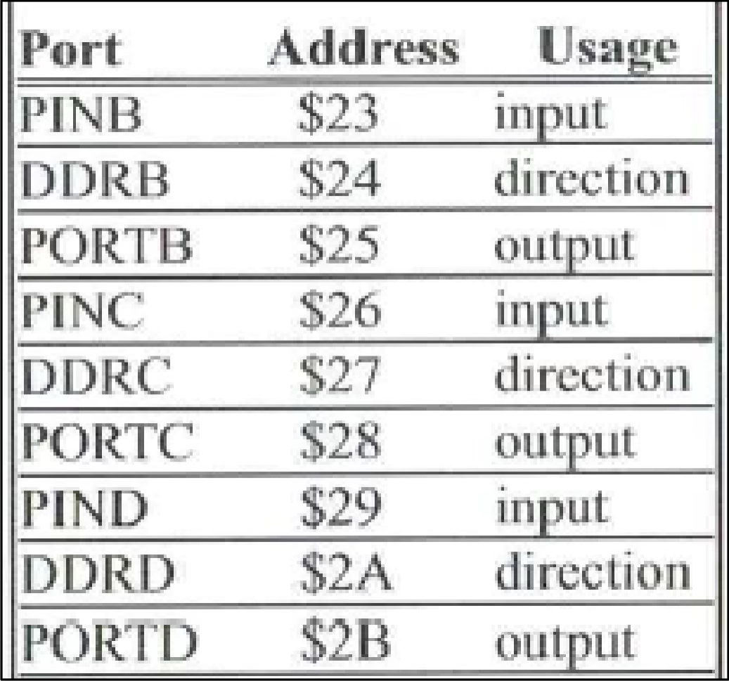
Setting Input/Output:
- Output Mode (
1in DDRx) → Value in PORTx is sent to the pin. - Input Mode (
0in DDRx) → Value from pin is stored in PINx register.
Output Port Programming
To allow the AVR to write a value to a pin (i.e., output pin) via Px0 – Px7, there are two steps:
- Declare an output pin by setting the bit in the ==DDRx register corresponding to this pin to 1. ==
- Write the value to this pin by setting the bit in the PORTx register corresponding to this pin.
Example
- Set the pin PB2 and PB4 as output pins. Set the output of PB2 to 0 and the output of PB4 to 1.
LDI R16, 0x14 OUT DDRB, R16 LDI R17, 0x10 OUT PORTB, R17 - Set all pins in Port D as output pins. Set PD0-PD2 to 0 and PD3-PD7 to 1.
LDI R16, 0xFF
OUT DDRD, R16
LDI R17, 0xF8
OUT PORTD, R17
Input Port Programming
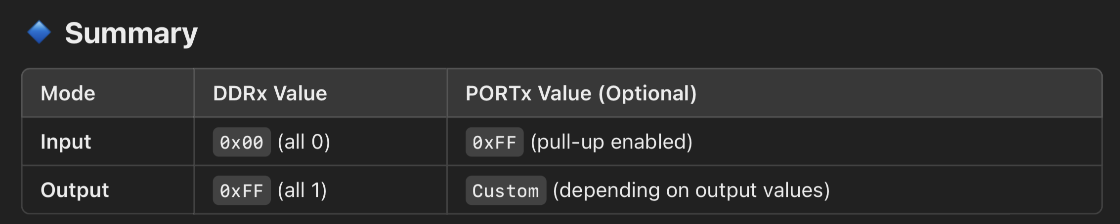
To allow the AVR to read a value from a pin (i.e., input pin) via Px0 – Px7, follow these three steps:
- Declare an input pin by setting the bit in the ==DDRx register corresponding to this pin to 0.==
- Set the bit in the PORTx register corresponding to this pin to 1.
- Read the value from this pin by reading the value from the bit in the PINx register corresponding to this pin.
Example: Set up Input Pins
- Set all pins in Port B as input pins. Read the values of the pins in Port B and store them in R18.
LDI R16, 0x00
OUT DDRB, R16
LDI R17, 0xFF
OUT PORTB, R17
IN R18, PINB
LDI R16, 0x00,OUT DDRB, R16→ Set all pins as input.LDI R17, 0xFF,OUT PORTB, R17→ Initialize Port B to 1.
I/O Bit Manipulation Instructions
I/O Bit Access Instructions
ATmega328 ports allow access to either all 8 bits or a single bit. The following instructions enable single-bit manipulation in any of the 64 I/O registers (not just port registers).

1. SBI (Set Bit in I/O Register)
Sets a specific bit in an I/O register to HIGH (1).
- Syntax:
SBI ioReg, bit_num - Parameters:
ioReg: I/O register name or address (3F$).bit_num: Bit position to set to 1.
- Example: Sets bit 5 in
PORTBhigh.SBI PORTB, 5
SBI PORTB, 5means you're specifically turning pin PB5 HIGH. ไม่ได้หมายความว่าตั้งตัวแปรอะไรให้มีค่าเป็น 5 นะ ทีแรกก็งง ๆ 5555 ==The bit number represents the pin index==
2. CBI (Clear Bit in I/O Register)
Clears a specific bit in an I/O register (sets it to LOW, 0).
- Syntax:
CBI ioReg, bit_num - Parameters:
ioReg: I/O register name or address (3F$).bit_num: Bit position to clear to 0.
- Example: Clears bit 2 in
PORTB.CBI PORTB, 2
3. SBIS (Skip if Bit in I/O Register is Set)
Skips the next instruction if the specified bit in the I/O register is HIGH (1).
- Syntax:
SBIS a, b - Parameters:
a: I/O register name or address (3F$).b: Bit position to check.
- Example: If bit 2 in
PINBis HIGH, it skipsRJMP AGAIN.AGAIN: SBIS PINB, 2 ; Skip if PB2 is HIGH RJMP AGAIN ; Keep checking if LOW
4. SBIC (Skip if Bit in I/O Register is Cleared)
Skips the next instruction if the specified bit in the I/O register is LOW (0).
- Syntax:
SBIC a, b - Parameters:
a: I/O register name or address (3F$).b: Bit position to check.
- Example: If bit 3 in
PINBis LOW, it skipsRJMP HERE.HERE: SBIC PINB, 3 ; Monitor PB3 for HIGH RJMP HERE ; Stay in the loop
SBISdoes not check for a specific number in the whole register. It only checks whether a single bit is 1 or 0.
Example 1
We connect a switch, an LED, and Rs to the Arduino UNO board according to the diagram below. We write and upload the following assembly program.
- What will happen to the LED if we press the switch?
- What will happen to the LED if we do not press the switch?
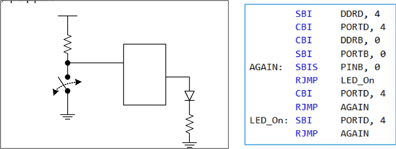
- Default แล้ว แต่ละรูจะมีไฟ 5 V หมายถึง 1 (Digital) เวลา Set ให้เป็น 0 มันก็จะต่อเข้า ground
Example 2
Assume that we connect a switch (similar to the previous example) to the pin PB2 of the Arduino UNO board. We write and upload the following assembly program.
- What will happen if we press the switch?
- What will happen if we do not press the switch?
    CBI     DDRB, 2       ; Clear bit 2 of DDRB (set PB2 as input)
    SBI     PORTB, 2      ; Set bit 2 of PORTB (enable pull-up resistor on PB2) (This line can be neglected)
    LDI     R16, 0xFF     ; Load immediate value 0xFF into register R16
    OUT     DDRD, R16     ; Set all bits of DDRD to 1 (configure PORTD as output)

AGAIN:
    SBIS    PINB, 2       ; Skip next instruction if bit 2 of PINB is set (button not pressed)
    RJMP    OVER          ; If button is pressed (bit 2 is 0), jump to OVER

    LDI     R16, 'Y'      ; Load ASCII value of 'Y' into R16
    OUT     PORTD, R16    ; Output 'Y' to PORTD
    RJMP    AGAIN         ; Repeat the loop

OVER:
    LDI     R16, 'N'      ; Load ASCII value of 'N' into R16
    OUT     PORTD, R16    ; Output 'N' to PORTD
    RJMP    AGAIN         ; Repeat the loop