#NotOnTheExam
Programmable Link Process Technologies
- Programmable logic devices are constructed using one of the following programmable link process technologies:
- Fuse — a metal link that connects a row and a column in the interconnection matrix. The link can be left intact, or it can be blown open by passing a sufficiently high current through it. Fuse technology is considered one-time programmable (OTP).

- Antifuse — opposite to a fuse link, an antifuse starts out with as two conductors separated by an insulator, such that no connection exists between a row and a column in the interconnection matrix. The link can be left as an open-circuit, or a sufficiently high voltage can be applied to the link such that the insulation breaks down and forms a low-resistance link. Antifuse technology is also OTP.

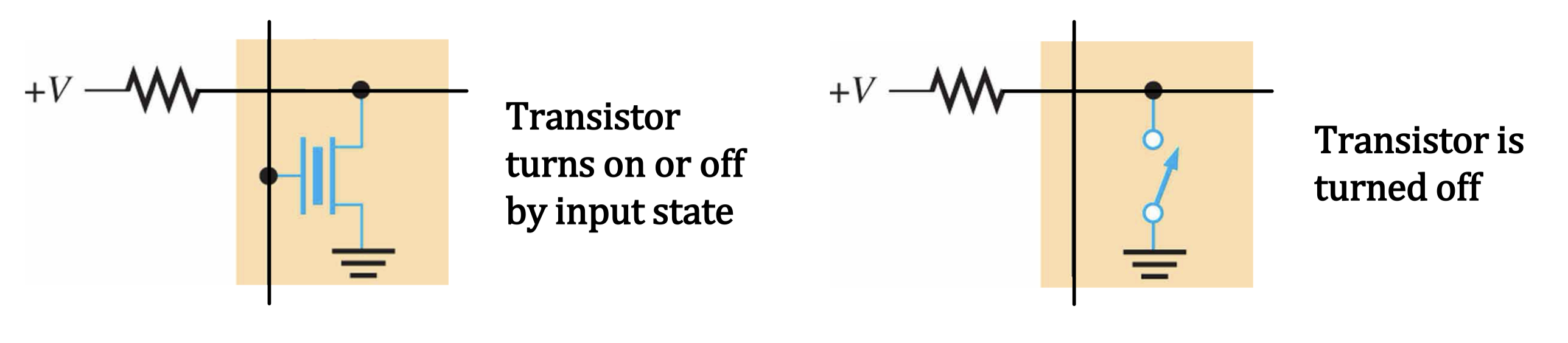
- EPROM and EEPROM — each link consists of an EPROM that uses a special type of MOSFET called the floating-gate transistor. The transistor is turned on (short-circuit) or off (open-circuit) by the input state, or it can be permanently programmed as off. Most EPROM-based devices are OTP, but some can be erased and reprogrammed, such as UV-EPROM and EEPROM.
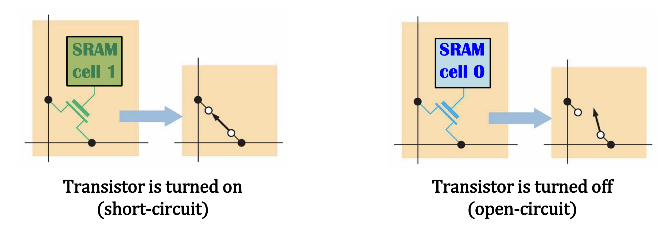
- SRAM — a SRAM-type memory cell is used to turn a transistor on or off to form a connection between a row and a column in the interconnection matrix. Unlike the other programmable link process technologies, SRAM technology is volatile and does not retain data when power is loss.
- Fuse — a metal link that connects a row and a column in the interconnection matrix. The link can be left intact, or it can be blown open by passing a sufficiently high current through it. Fuse technology is considered one-time programmable (OTP).
Programmable Logic: SPLD
- Simple programmable logic device (SPLD) comes in two major types:
- PAL (programmable array logic).
- GAL (gated array logic).
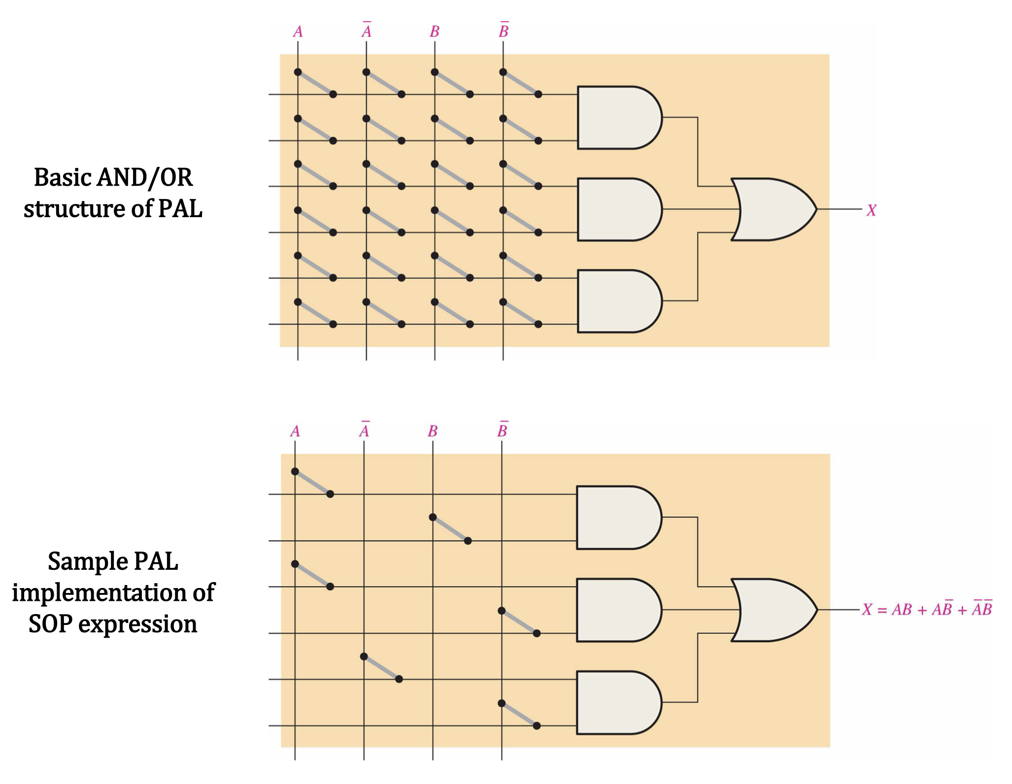
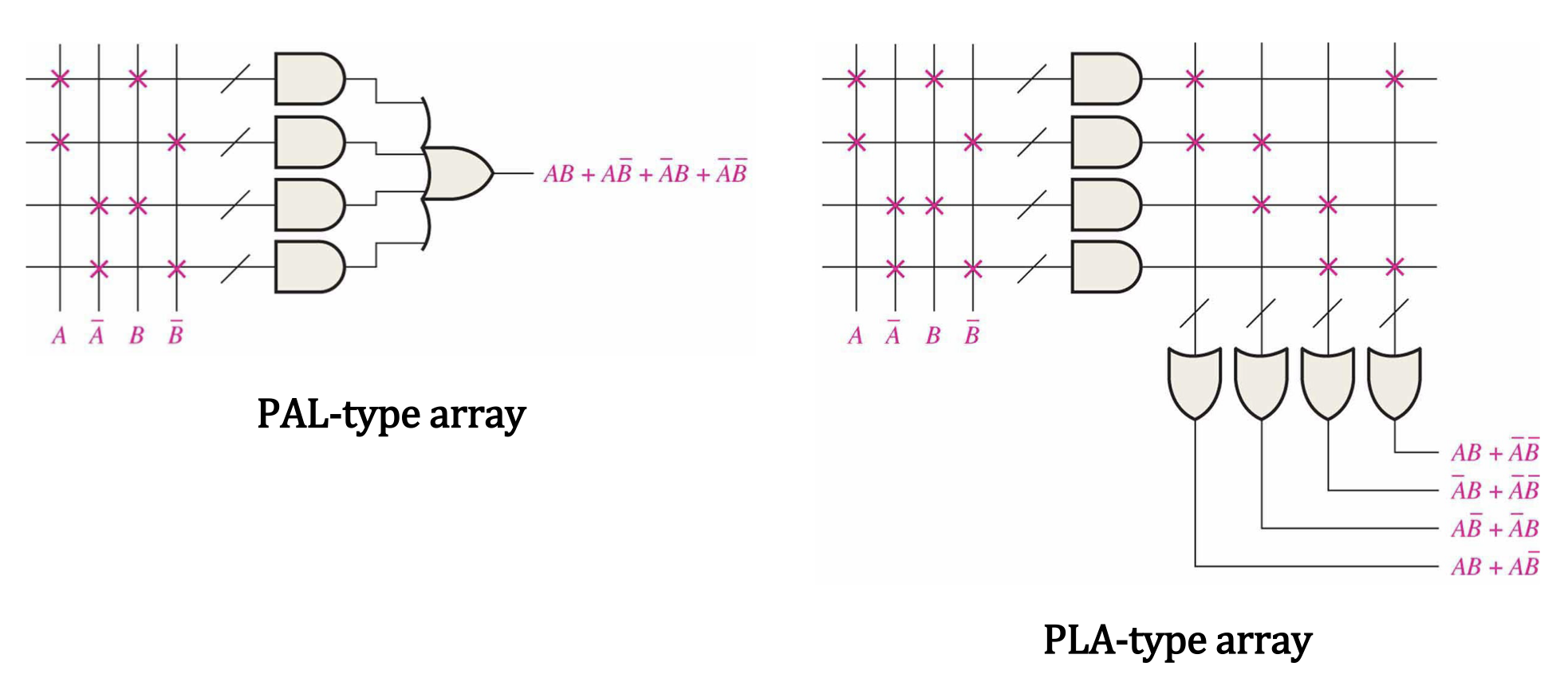
- The PAL is a programmable array of AND gates that connects to a fixed array of OR gates. Generally, PALs are implemented with fuse process technology and are one-time programmable (OTP).
- The structure of PALs allow any SOP logic expressions with a defined number of variables to be implemented. Remember that any combinational logic function can be expressed in SOP form!
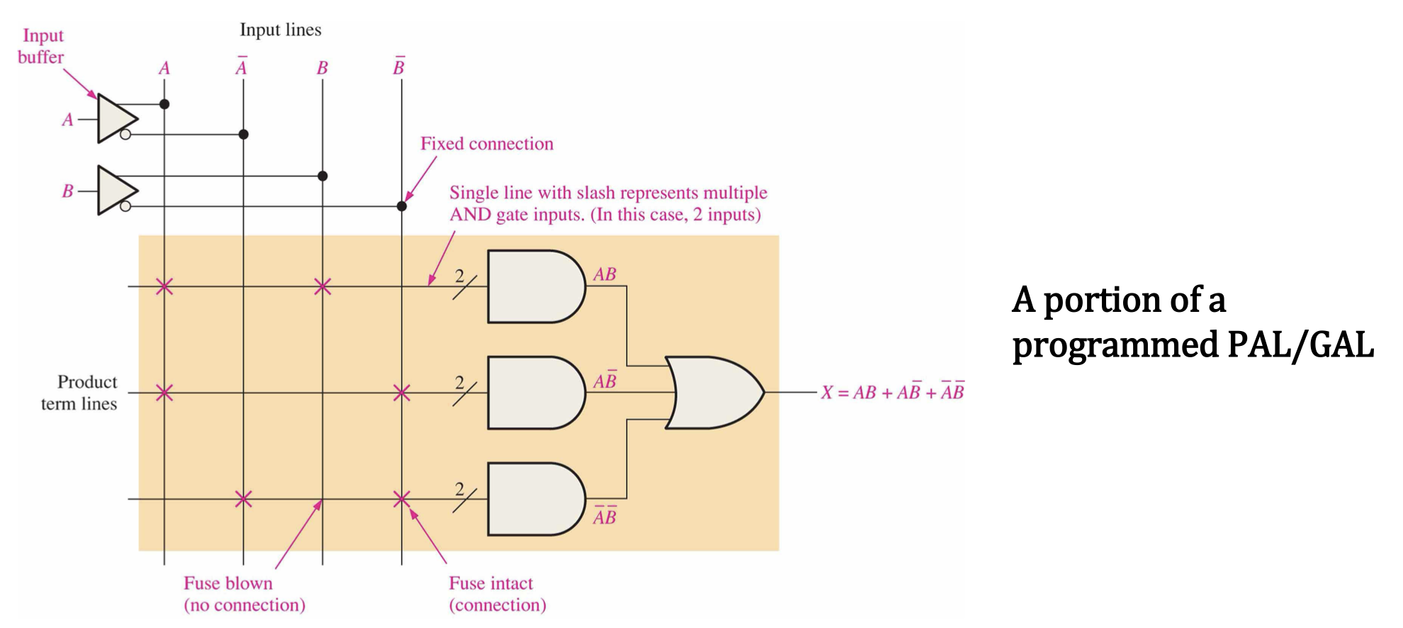
- PALs contain a grid or matrix of conductors that form rows and columns with a programmable link (fuse) at each cross point (also called a cell).
- Each row is connected to the input of an AND gate, and each column is connected to aninput variable or its complement.
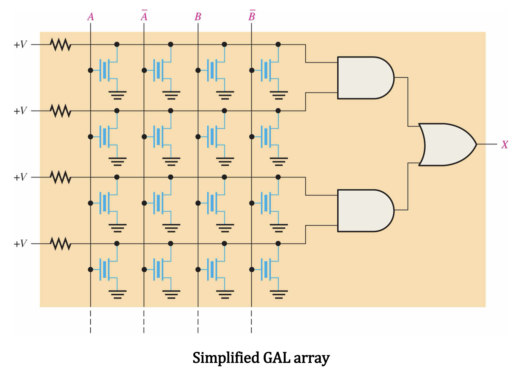
- The GAL is essentially a PAL that can be reprogrammed, with the same type of AND/OR organization.
- The main difference is that the GAL uses areprogrammable process technology, such as EEPROM (E2CMOS) instead of fuses.
Simplified Notation
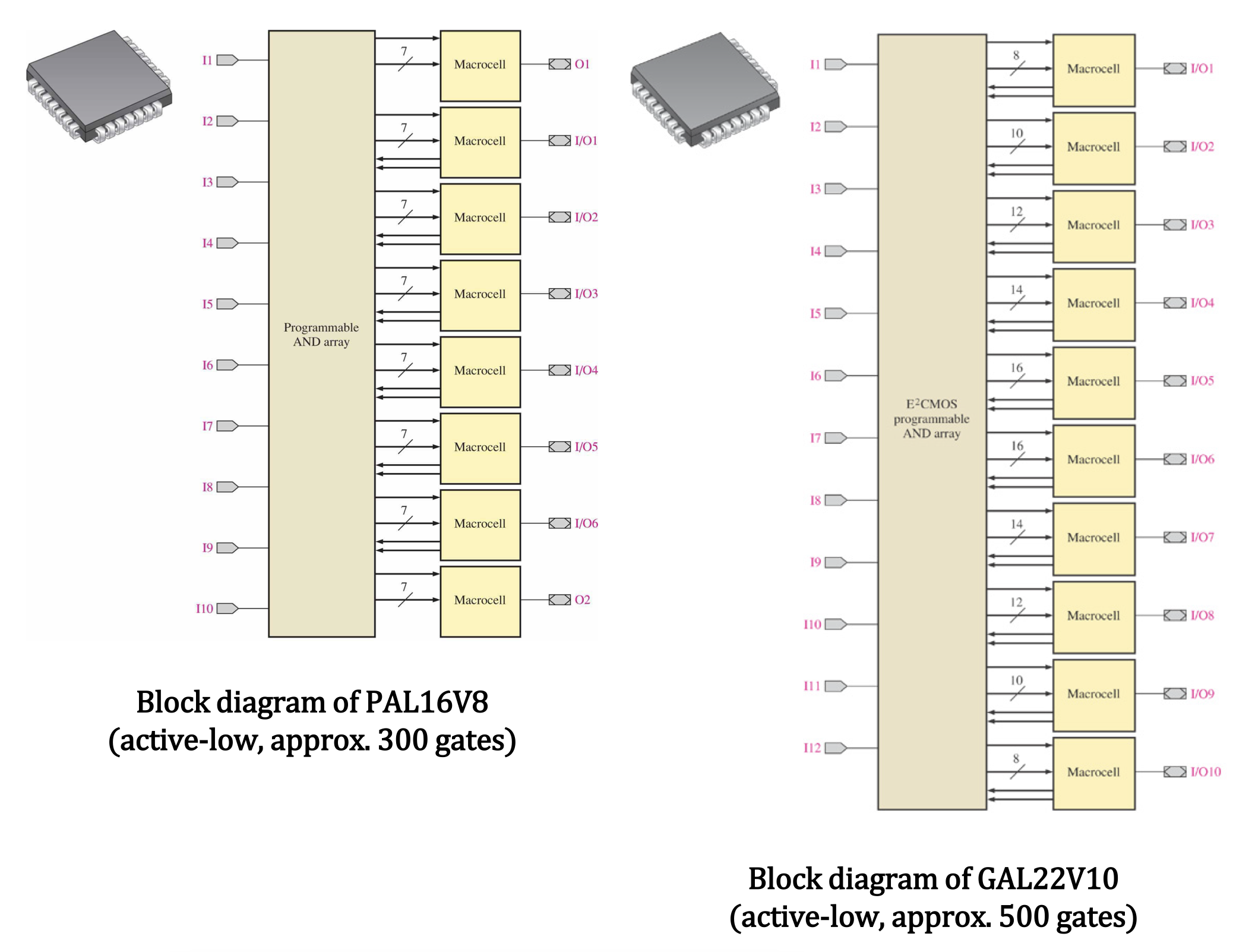
- Actual PAL and GAL devices contain many AND and OR gates in addition to other elements, and are capable of handling many variables and their complements.
- They are often represented by simplified diagrams such as the one below. Notice the presence of a buffer at the inputs to preventing loading by a large number of AND gate inputs to which they are connected.
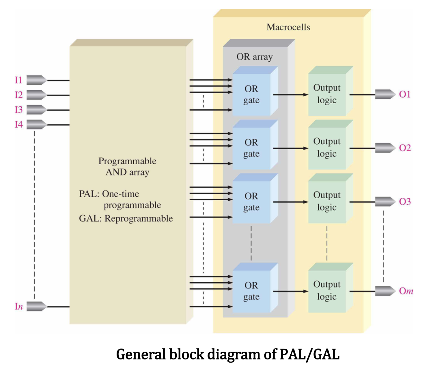
General Block Diagram
- The right figure illustrates a general block diagram of a PAL/GAL.
- A macrocell generally consists of one OR gate and some associated output logic.
- The complexity of the macrocell depends on the type of PAL/GAL, and can be configured for combinational logic or registered logic (with flip-flops), or both.
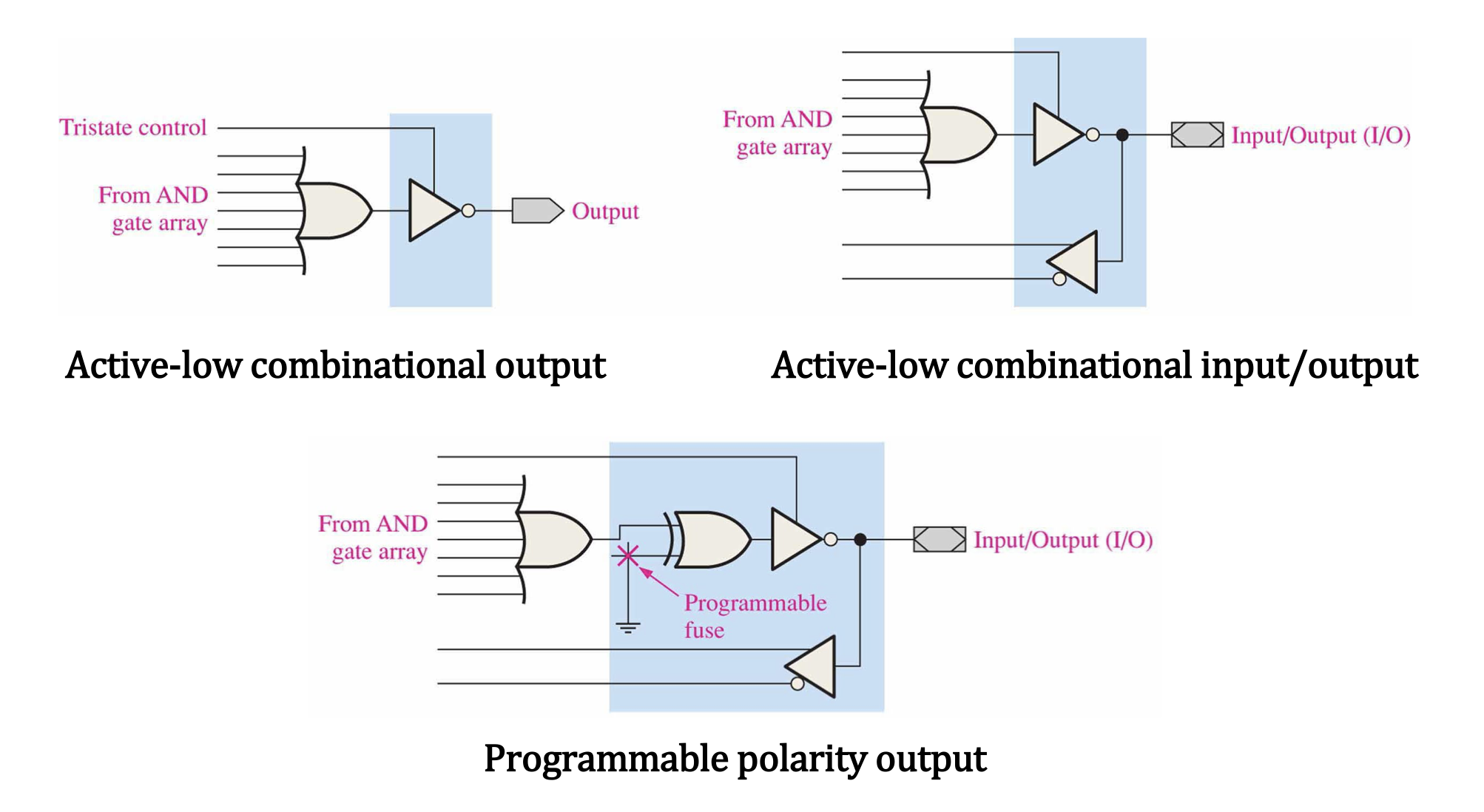
- The above figures contain some examples of different combinational logic macrocells.
- Notice the use of inverter withtristate control, which can make the inverter act like an open circuit to completely disconnect the output.
- Figures (b) and (c) show how a macrocell can be used as both an input or output. Figure (c) can be programmed as either active-LOW or active-HIGH output.
Programmable Logic Array
- Some manufactures, such as Xilinx, employ a programmable logic array (PLA) structure instead of PAL/GAL.
- While a PAL has a programmable AND array followed by a fixed OR array, the PLA has a programmable AND array followed by a programmable OR array.
Programmable Logic: CPLD
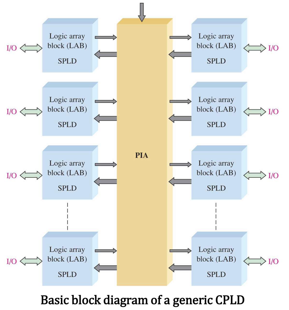
- Complex programmable logic devices (CPLD) consist of multiple SPLD arrays with programmable interconnections.
- Each SPLD array is called a logic array block (LAB), function block, logic block, or generic block.
- The programmable interconnections are called programmable interconnect array (PIA) or advanced interconnect matrix (AIM).
- This allows for the construction of very complex logic circuits basedon the SOP structure of individual LABs.
📄 EES 271-13 PLD and VHDL pages 13 - 18.pdf
Programmable Logic: FPGA
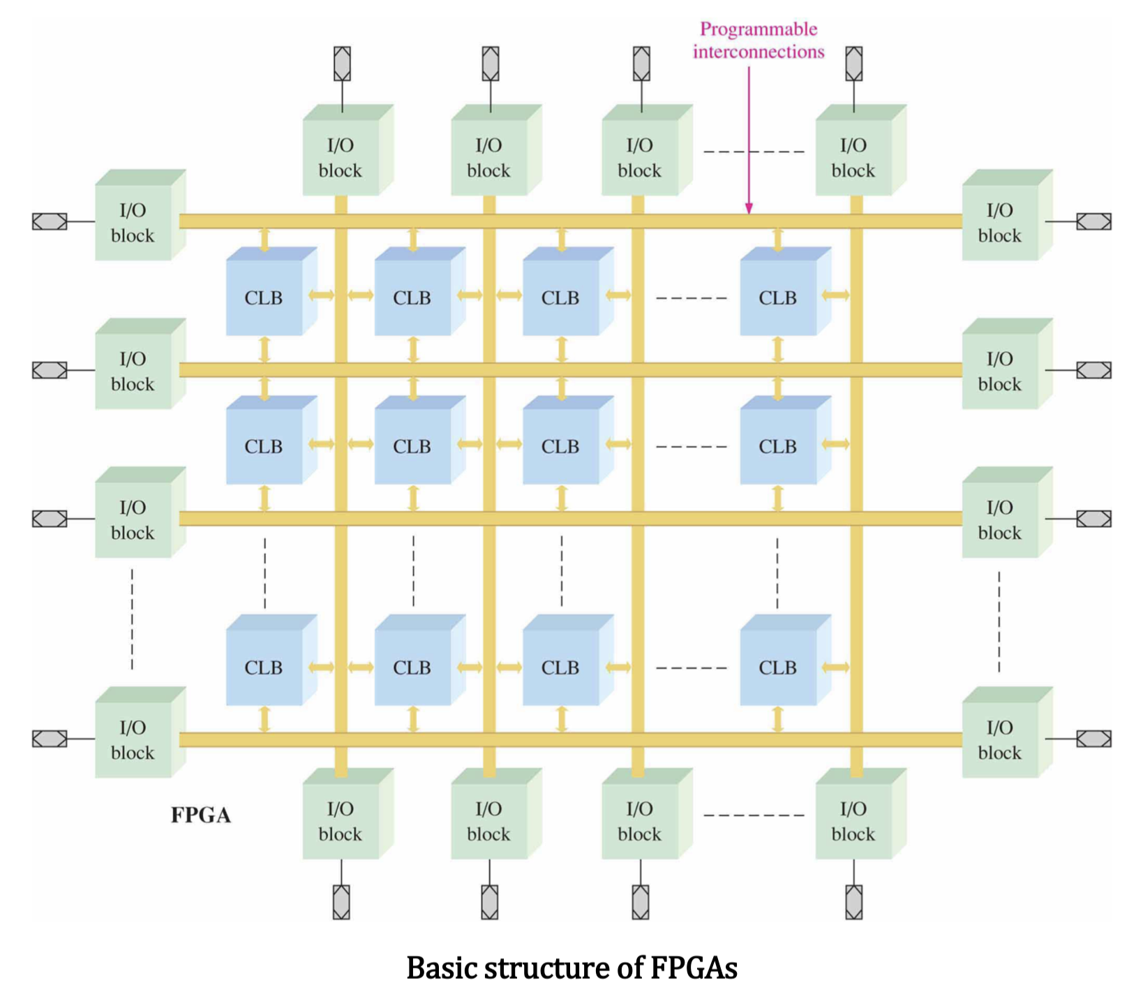
- A more powerful version of PLDs is thefield-programmable gate array (FPGA), which does not use PAL or PLA, and has a much greater density than CPLDs. This is because of smaller logic-producing elements.
- The FPGA consists of three basic components:
- Configurable logic blocks (CLBs) ~ not as complex as LABs or FBs in CPLDs, but there is generally more of them. When the CLBs are simple, the FPGA architecture is called fine-grained. When it is larger and more complex, it is called coarse grained.
- Programmable interconnections ~ arranged into a distributed matrix (rows and columns).
- I/O blocks ~ located around the device, providing individually selectable input, output, or bidirectional connections to the outside world.
- Most programmable logic manufacturers make FPGAs that range in density, power consumption, supply voltage, speed, and architecture.
- FPGAs are reprogrammable and use SRAM or antifuse process technology.
Configurable Logic Blocks
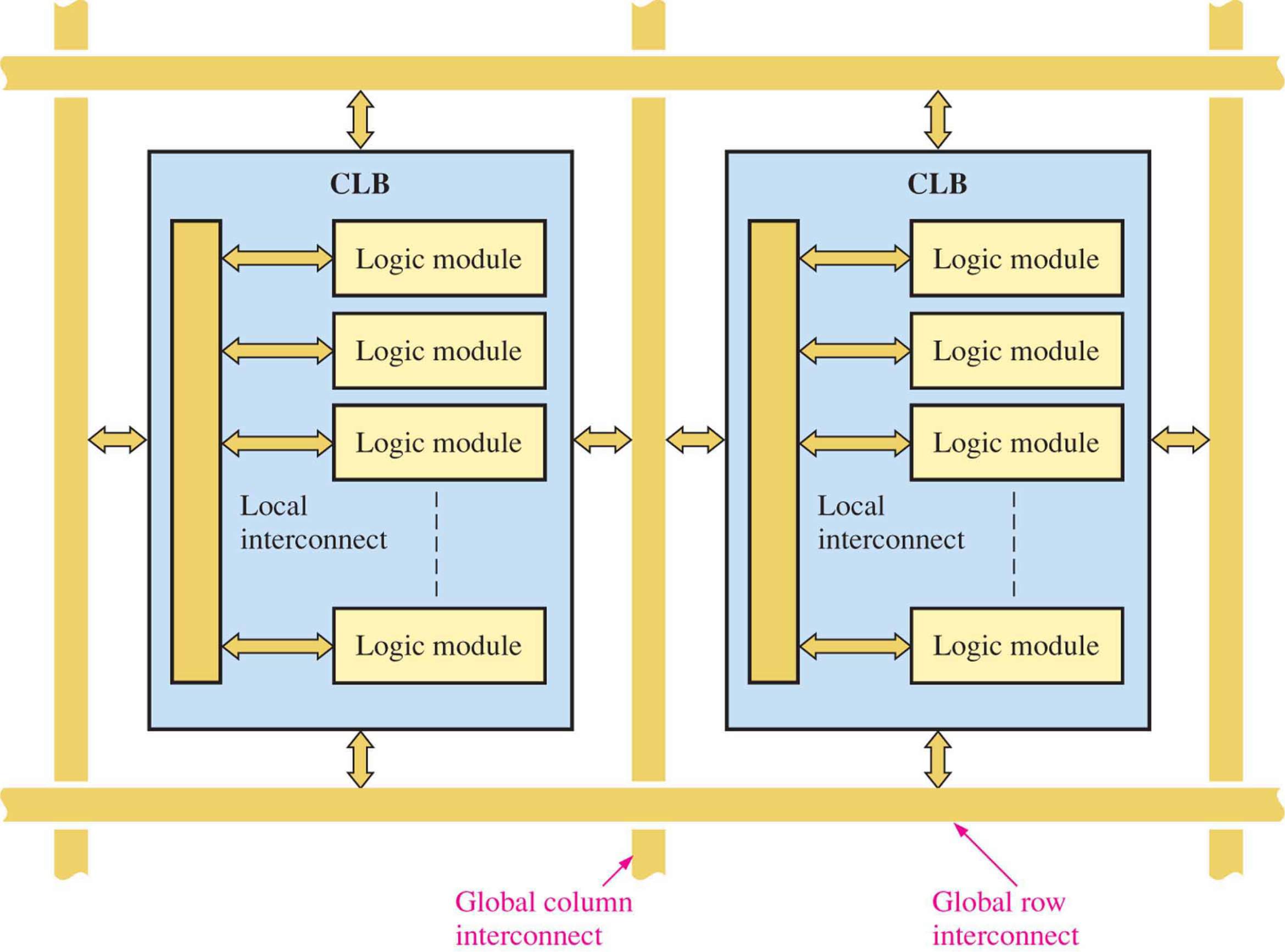
- A FPGA logic block consists of several smaller logic modules that are the basic building units (similar to macrocells in CPLDs).
- Each CLB is made up of multiple smaller logic modules and alocal programmable interconnect that is used to connect logic modules within the CLB.
Logic Modules
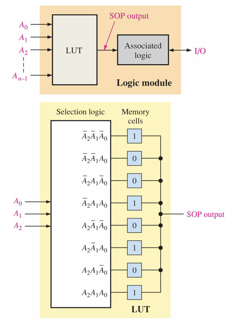
- A logic module in an FPGA logic block can be configured for combinational logic, registered logic, or a combination of both.
- A flip-flop is part of the associated logic and is used for registered logic.
- It employs a look-up table (LUT), which is a type of memory that is programmable and used to generate SOP combinational logic functions. The LUT performs the same function as the PAL or PLA.
- Generally, the LUT consists of a number of memory cells equal to 2n, where n is the number of input variables.
- SRAM-based FPGAs are volatile (data programmed into the CLBs are lost when power is turned off).
Programmable Logic Software
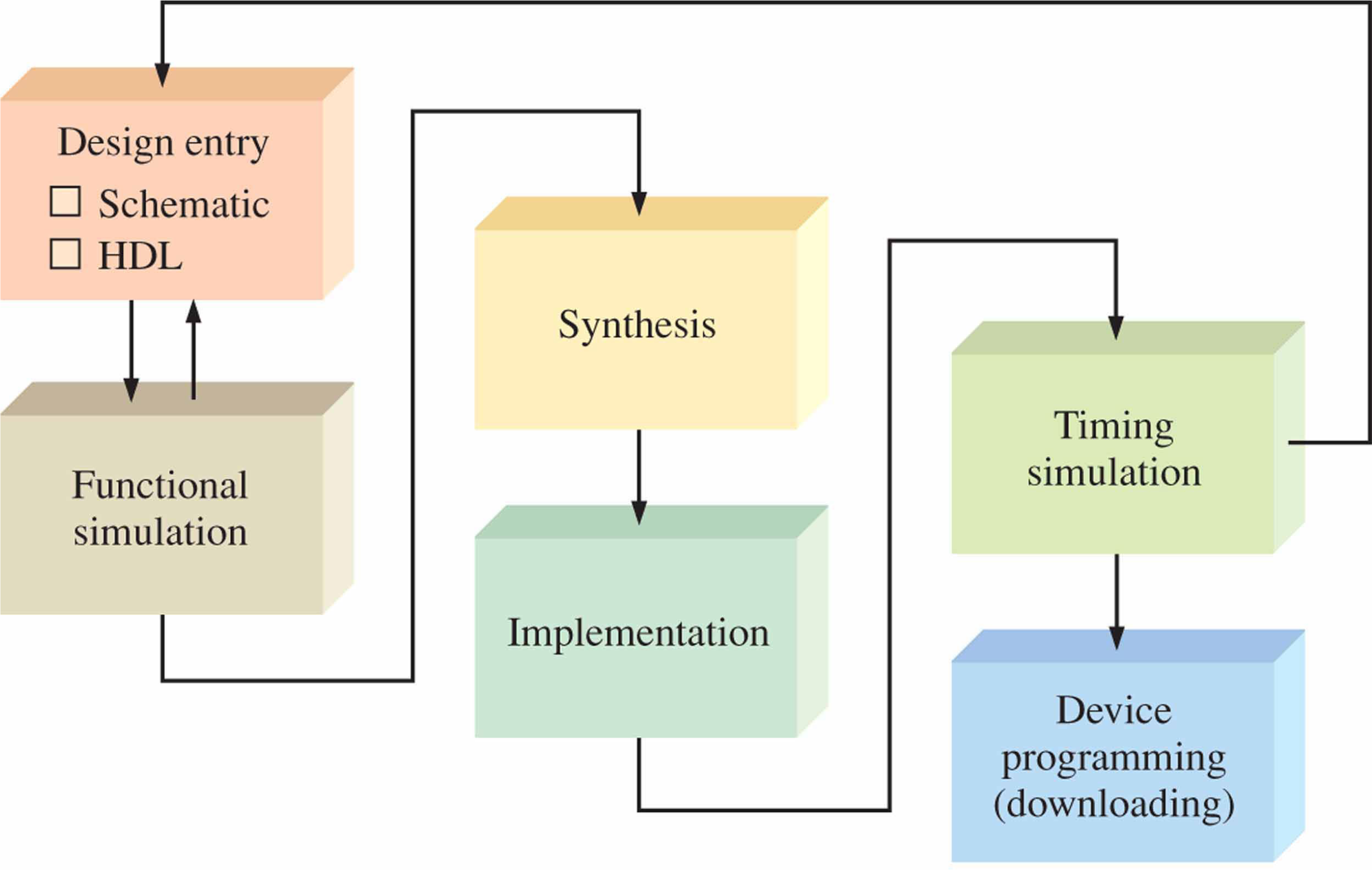
- In order to program a PLD, you must use a programmable logic software, which can either be schematic entry or text entry.
- The programming process is generally referred to as design flow. A basic define flow diagram for implementing a logic design is shown below.
- The device being programmed is usually referred to as the target device.
Design Entry
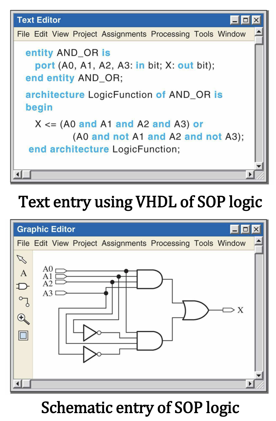
- The design entry refers to the process of entering your design into the computer, using either schematic entry or text entry.
- In order to use text entry, you must know how to program using hardware description languages (HDLs), such as VHDL (VHSIC hardware description language) or Verilog. Truth tables can also be accepted as a text-based input.
- Schematic entry allows you to place symbols of logic gates and other logic functions, and connect them as required by your design.
Introduction to VHDL
- As mentioned previously, VHDL (VHSIC hardware description language) is a text-based method for programming your PLDs that allows you to implement SOP Boolean expressions.
- When using VHDL, several rules should be followed:
- Comment lines start with the double hyphen
--. - VHDL is case insensitive.
- While the expressions such as
c <= NOT s;is called the data flow description, there is another way of defining an operation called the behavioral description that allows us to type asIF s = ‘0’ THEN c<= ‘1’ ELSE c <= ‘0’ END IF.
- Comment lines start with the double hyphen
- For a more detailed discussion of VHDL, please refer to the following references:
Example VHDL code of a half-adder
library IEEE;
use IEEE.std_logic_1164.all;

entity HalfAdderTrial2 is port (

	A : in std_logic;
	B : in std_logic;
	Sum: out std_logic;
	Cout : out std_logic );

end entity HalfAdderTrial2;

architecture Arch1 of HalfAdderTrial2 is
begin

	Sum <= A xor B;
	Cout <= A and B;

end architecture Arch1;
Example VHDL code of a NAND gate
library IEEE; -- Declaration of the use of the IEEE library
use IEEE.std_logic_1164.all; -- Declaration of the use of IEEE 1164 package

-- Definition of inputs and outputs

entity NAND_gate is -- Name the function as NAND gate
port (
    A : in std_logic;
    B : in std_logic;
    C : out std_logic;
    Cout: in std_logic );
end entity NAND_gate;

architecture LogicFunction of NAND_gate is
    signal S : std_logic; -- Internal signal
begin
    S <= A and B; -- Definition of the logic
    C <= not S; -- <= is a signal assignment operator
end architecture LogicFunction;
Example VHDL code of synchronous counter with asynchronous reset
library IEEE;
use IEEE.std_logic_1164.all;
use IEEE.numeric_std.all;

entity Counter is
    generic (
        WIDTH : in natural := 32);
    port (
        RST : in std_logic;
        CLK : in std_logic;
        LOAD : in std_logic;
        DATA : in std_logic_vector(WIDTH-1 downto 0);
        Q : out std_logic_vector(WIDTH-1 downto 0) );
end entity Counter;

architecture RTL of Counter is
begin
    process(all) is
    begin
        if RST then
            Q <= (others => '0');
        elsif rising_edge(CLK) then
            if LOAD then
                Q <= DATA;
            else
                Q <= std_logic_vector(unsigned(Q) + 1);
            end if;
        end if;
    end process;
end architecture RTL;