Conditional Loop Instructions
AVR Status Register
- The AVR microcontroller includes a flag register that indicates arithmetic statuses, such as the carry bit.
- This flag register is called the Status Register (SREG), consisting of 8 bits.
- It is located at memory address (or equivalently, the I/O address ).
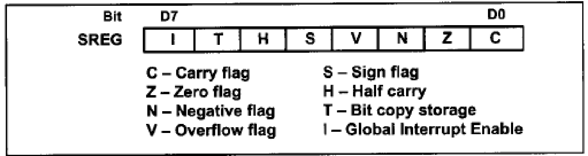
- Each flag bit is either 0 (false) or 1 (true) and is updated after an arithmetic instruction (e.g.,
ADD,SUB,INC,DEC). More details can be found in Chapter 5 of the textbook.
Explanation of Flags
-
Carry Flag (C):
- → No carry bit.
- → Carry bit exists.
Think of this like an overflowing cup. If water spills over, you have a carry (C = 1). If it doesn’t, no carry (C = 0).
-
Zero Flag (Z):
- → The result is nonzero.
- → The result is zero.
Like checking if your wallet is empty: if there's money (), you're not broke; if there’s nothing inside (), you are.
-
Negative Flag (N):
- → The result is not negative.
- → The result is negative.
Imagine checking your bank balance: if it’s positive (), you have money. If it's negative (), you’re in debt.
-
Overflow Flag (V):
- → No overflow.
- → Overflow occurred.
Like a speedometer: if it goes beyond the max speed it can display, you have an overflow.
-
Sign Flag (S):
- Defined as (XOR operation between N and V).
-
Half Carry Flag (H):
- → No carry from bit D3 to D4.
- → Carry from bit D3 to D4.
Instructions That Affect SREG
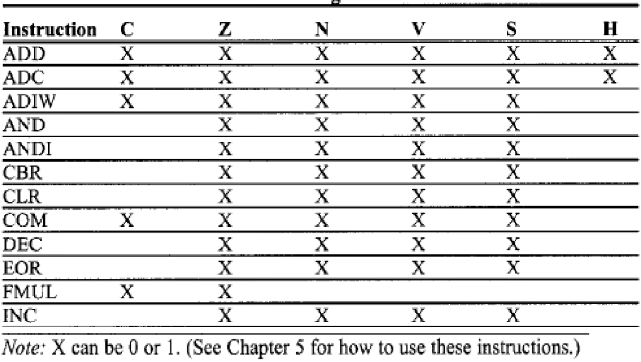
- The status register is modified by various arithmetic and logic operations.
- Below is a list of example instructions that impact the status register:
Conditional Branch Instructions
- Branch refers to jumping to a program-memory address specified by a label.
- A branch instruction updates the program counter to a target program address.
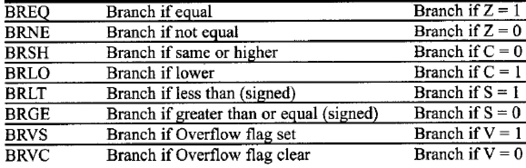
- The table below lists conditional branch instructions in AVR assembly. These instructions jump only if a condition (based on status flags like C, Z, N, V) is met.
Examples of Conditional Branch Instructions
- BRNE (Branch if Not Equal to Zero): Jumps if .
- Example:
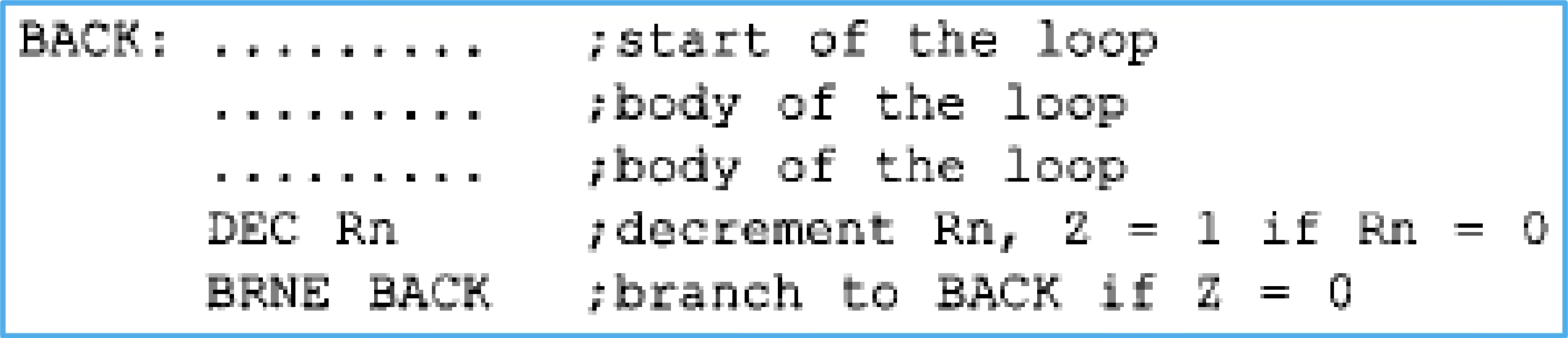
- Example:
- BREQ (Branch if Equal to Zero): Jumps if .
- Example:

- Example:
All Conditional Branches are Short Jumps
-
A branch instruction determines the target address using a relative address, which is the difference between the program counter’s current value and the target address.
-
All conditional branches are short jumps, meaning ==the target must be within -64 (backward) to +63 (forward) from the current program counter value.==
-
Reason for short jumps is illustrated below:
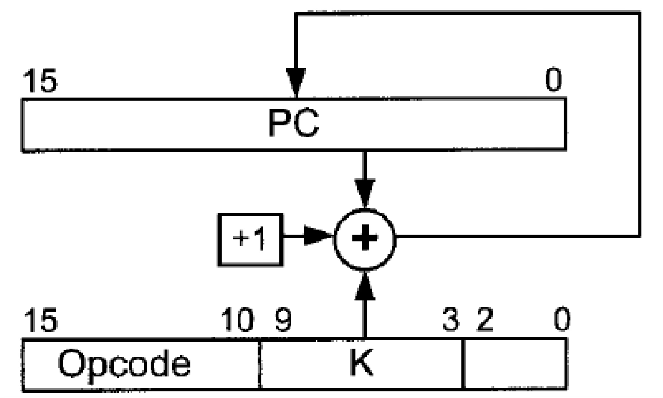
- All conditional branch instructions are 2-byte instructions.
- The opcode is a 6-bit binary number (D10 – D15), and the relative address is a 7-bit binary number (D3 – D9).
- Since the relative address is 7-bit, the range is -64 to +63.
Imagine you can only jump a limited distance in a game. If the next platform is too far, you need another way to reach it.
Unconditional Branch Instructions
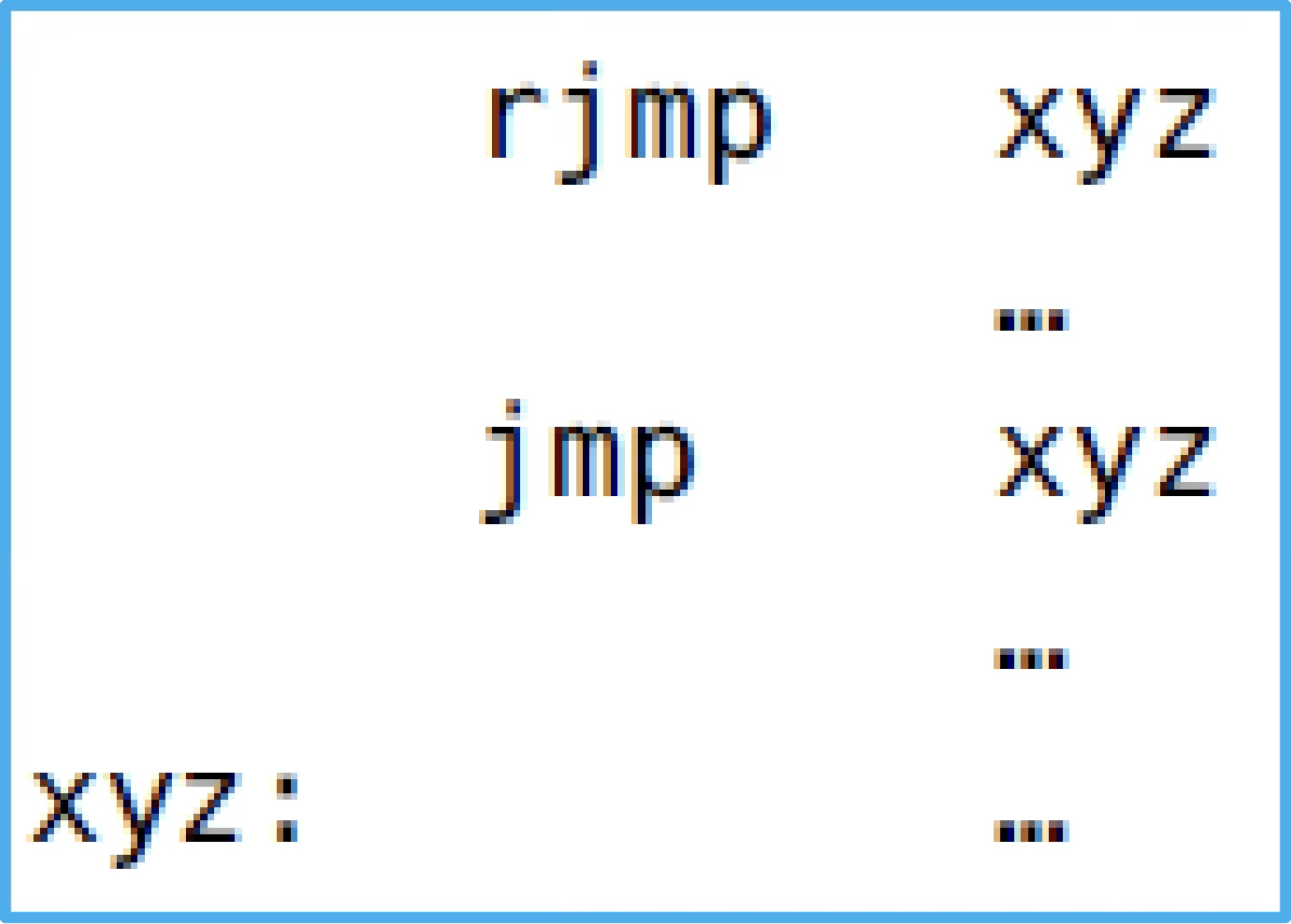
- AVR assembly includes three unconditional branch instructions: JMP, RJMP, and IJMP. This section focuses on JMP and RJMP:
- JMP (Jump): Unconditional jump to any memory location. 4-byte instruction.
- RJMP (Relative Jump): Unconditional jump within -2048 to +2047 of the current program counter. 2-byte instruction.
- Example:
Think of
JMPlike teleporting anywhere on a map, whileRJMPis like dashing a short fixed distance forward or backward.
Stack and Stack Pointers
Stack and Stack Pointer
The stack is a section of data memory used to store information temporarily, such as data or addresses. The stack pointer (SP) is a 2-byte register that stores the data address where information will be placed. It consists of two registers in I/O memory:
- SPH (Stack Pointer High) - Address: $5E
- SPL (Stack Pointer Low) - Address: $5D
The address stored in SP ranges from FFFF.

Stack – Storing and Retrieving Information
The stack follows a Last-In, First-Out (LIFO) approach, similar to how Swift manages function calls using the stack in iOS development. Data is stored and retrieved via a General Purpose Register (GPR).
Pushing into the Stack (PUSH Instruction)
The PUSH instruction stores data from a GPR into the stack at the address specified by SP and then ==decrements SP by 1 automatically.==
PUSH Rr ; Rr can be any of the general purpose registers (R0-R31)Example:
PUSH R10 ; Store R10 onto the stack, and decrement SPPopping from the Stack (POP Instruction)
The POP instruction retrieves data from the stack (at the address specified by SP), loads it into a GPR, and then ==increments SP by 1 automatically.==
POP Rr ; Rr can be any of the general purpose registers (R0-R31)Example:
POP R16 ; Increment SP, then load the top of stack into R16Initializing the Stack Pointer
When an AVR microcontroller powers up, the stack pointer (SP) may initially contain **0000 - $0060), SP must be initialized to a safe location.
Key Points:
- The stack grows downward from a higher memory address to a lower memory address (LIFO principle).
- SP is set to the uppermost data memory location (the last data memory address).
- For ATmega328, the last stack address is $08FF, considering that its total data memory (including GPRs, I/O registers, and SRAM) is 2304 Bytes.
Setting Up the Stack Pointer
To initialize SP correctly, we load the high byte of RAMEND into SPH and the low byte of RAMEND into SPL.
Example
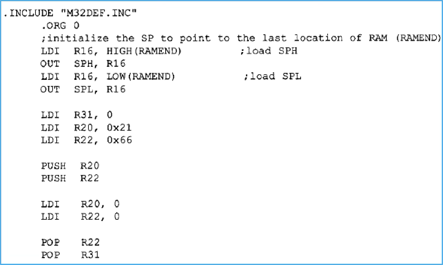
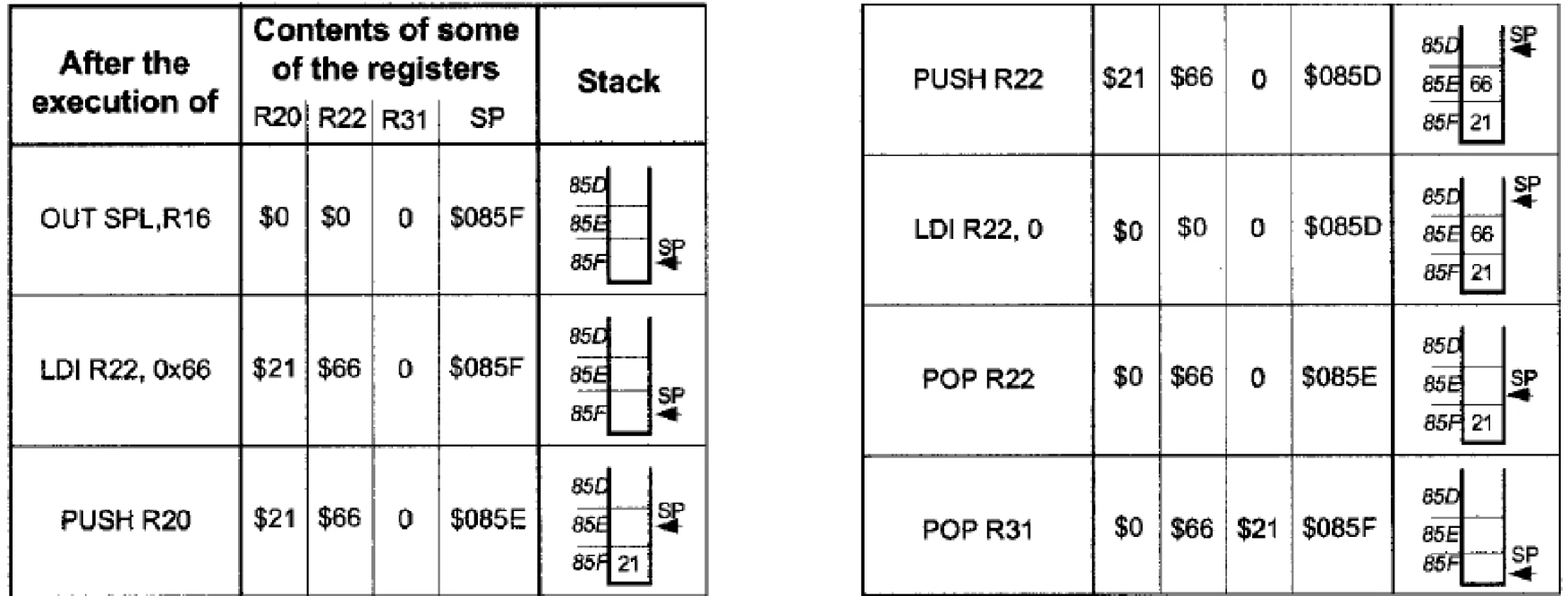
- This example shows how the stack and the stack pointer work. For this example, assume that the last data memory address is $085F.
Subroutines and Call Instructions
Subroutines and Call Instructions
A subroutine (or function) is a set of instructions that may be used repeatedly. Instead of writing the same instructions multiple times, we define them separately and use the CALL instruction to invoke them.
CALL Instruction
- The CALL instruction is a 4-byte instruction that calls a subroutine.
- When using CALL, the program counter (PC) (which holds the current instruction address) is pushed onto the stack.
- ==The low byte is pushed first, followed by the high byte.==
- This allows the AVR to return to the correct address after the subroutine executes.
- The address stored in the PC is the next instruction’s address (current instruction +1).
RET Instruction
- Every subroutine must end with a
RETinstruction. - The
RETinstruction tells the AVR where to return in the main program. - When
RETis executed:- The top two bytes from the stack are popped back into the PC.
- The program resumes execution at the stored return address.
Example: Calling a Subroutine
Below is an example using CALL to invoke a DELAY subroutine, assuming the last data memory address is $085F.
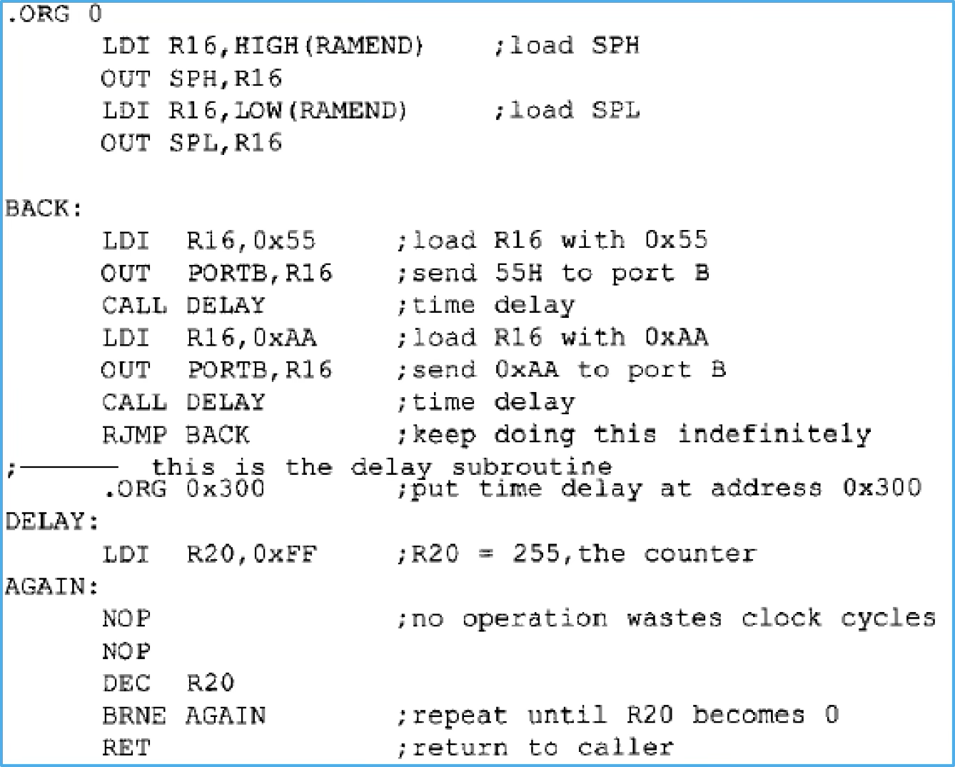
Stack Analysis for CALL and RET
The stack behavior when using CALL and RET is as follows:
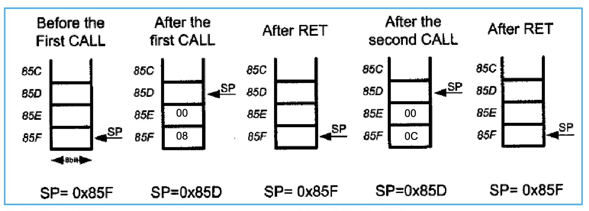
This mechanism is similar to how Swift functions operate—when a function is called, the return address is pushed onto the stack, and when the function exits, the return address is popped, ensuring proper execution flow.
AVR Time Delay Summary
Instruction Cycle
- An instruction cycle consists of fetch, decode, and execute stages
- Duration = 1/(crystal frequency)
- Examples:
- 8MHz → 0.125μs (125ns)
- 16MHz → 0.0625μs (62.5ns)
- 10MHz → 0.1μs (100ns)
- 1MHz → 1μs
Instruction Cycle Requirements
- Different instructions require different numbers of cycles to complete
- This affects execution time of each instruction
Time Delay Computation
- Used when program needs to pause temporarily
- Created by loops that repeat a set of instructions
- Total delay calculation is essential for timing applications
Example: Loop Delay Example
DELAY:  LDI R20, 0xFF ; 1 cycle
AGAIN:  NOP           ; 1 cycle
        NOP           ; 1 cycle
        DEC R20       ; 1 cycle
        BRNE AGAIN    ; 2 cycles (1 cycle on final iteration)
        RET           ; 4 cycles
With 1MHz clock (1μs per cycle):
- Initial load: 1 cycle
- Loop (255 iterations × 5 cycles per iteration): 1275 cycles
- Final iteration BRNE: -1 cycle (only takes 1 not 2)
- Return: 4 cycles
Total delay:
Example: Delay from a Nested Loop
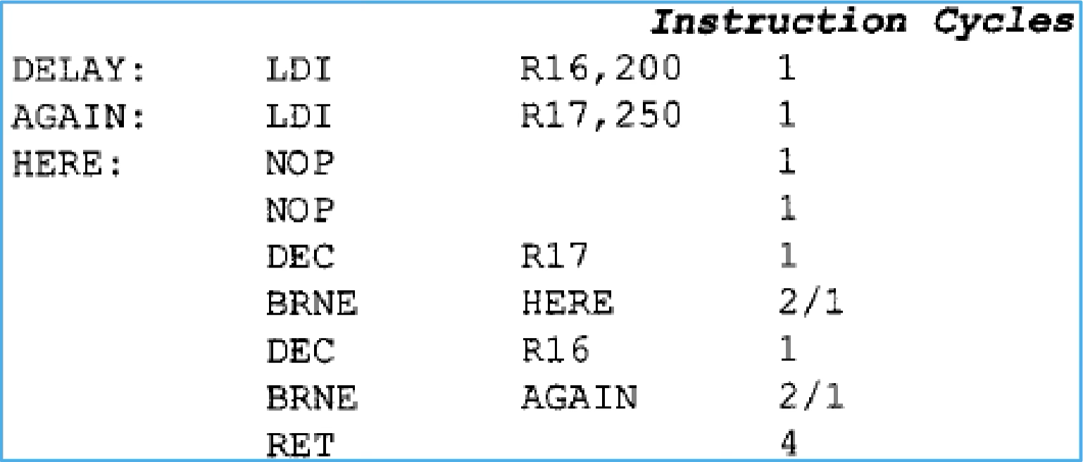
- Assume the crystal frequency is 1 MHz. Compute the time delay from this DELAY subroutine.
DELAY:  LDI R16, 200 ; 1 cycle
AGAIN:  LDI R17, 250 ; 1 cycle
HERE:   NOP          ; 1 cycle
        NOP          ; 1 cycle
        DEC R17      ; 1 cycle
        BRNE HERE    ; 2 cycles (1 cycle on final iteration)
        DEC R16      ; 1 cycle
        BRNE AGAIN   ; 2 cycles (1 cycle on final iteration)
        RET          ; 4 cycles
Formula for Nested Loop Delay
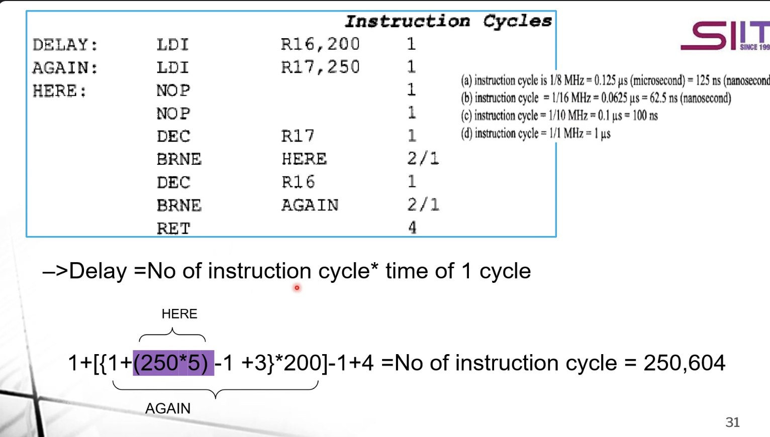
For nested loops, we need to account for both the inner and outer loop execution patterns. The total number of instruction cycles can be calculated as:
Where:
- Initial Setup: Initial instructions before entering loops
- Outer Loop: Instructions in outer loop × number of iterations
- Final Return: Instructions after all loops complete
For this specific example:
- Initial LDI R16,200: 1 cycle
- Outer loop (AGAIN):
- LDI R17,250: 1 cycle
- Inner loop (HERE) complete execution: [1+1+1+2+1+3]×250 - 1 = 5×250 - 1 = 1249 cycles
- DEC R16: 1 cycle
- BRNE AGAIN: 2 cycles (1 cycle on final iteration)
- Final RET: 4 cycles
The calculation formula matches what's shown in the image:
Generalized Formula
For a nested loop with counters N (outer) and M (inner):
Where:
- Setup: Initial instructions
- Inner Setup: Instructions before inner loop
- Inner Body: Instructions in inner loop body
- Post Inner: Instructions after inner loop
- Final: Instructions after all loops complete
This provides the total number of instruction cycles, which can be multiplied by the cycle time (based on crystal frequency) to get the actual delay in time units.